SocketModem® MTQ User Guide
Models: MTQ-L1G2D-B02, MTQ-L4G1-B02, MTQ-LNA7-B02, MTQ-LEU7-B02, MTQ-LAT3-B01, MTQ-LAT3-B02, MTQ-MNG6-B02
Document Part Number: S000843 Rev. 1.0
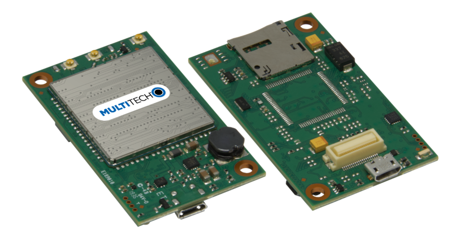
About the SocketModem® MTQ
SocketModem® MTQ embedded cellular modems are complete, ready-to-integrate communications devices ideal for customers looking to add 4G-LTE cellular communications to their IoT/M2M solutions. These communications devices enable easy technology transitions and allow developers to add wireless communication to products with a minimum of development time and expense. SocketModem MTQ modems are carrier approved and end-device certified, decreasing time to market while saving customers money.
The SocketModem MTQ maintains interoperability with legacy systems that use a 40-pin connector and forward mounting hole. All SocketModem MTQ software is open source.
Build Options
| Ordering Part Number | Description | Region |
|---|---|---|
| MTQ-L1G2D-B02 | Embedded LTE Cat 1 Modem with Fallback and GNSS (50 pack) |
Australia Canada European Union United Kingdom United States |
| MTQ-L1G2D-B02-SP | Embedded LTE Cat 1 Modem with Fallback and GNSS (single pack) | |
| MTQ-L4G1-B02 | Embedded LTE Cat 4 Modem with Fallback and GNSS (50 pack) | |
| MTQ-L4G1-B02-SP | Embedded LTE Cat 4 Modem with Fallback and GNSS (single pack) | |
| MTQ-LNA7-B02 | Embedded LTE Cat 4 Modem with Fallback and GNSS (50 pack) |
Canada United States |
| MTQ-LNA7-B02-SP | Embedded LTE Cat 4 Modem with Fallback and GNSS (single pack) | |
| MTQ-LEU7-B02 | Embedded LTE Cat 4 Modem with Fallback |
Australia European Union United Kingdom |
| MTQ-LEU7-BO1 | LTE Cat. 4 - SOM Version |
European Union United Kingdom |
| MTQ-LEU7-BO2 | LTE Cat 4 | |
| MTQ-MNG6-B02 | Embedded LTE Cat M1 with GNSS and 2G fallback |
Australia Canada European Union United Kingdom United States |
| MTQ-MNG6-B02-SP | LTE Cat M1 SoM with GNSS (single pack) |
- Devices ship without network activation. To connect devices to the cellular network, contact your service provider and request the correct SIM cards.
- The complete ordering part number may include an "Rx" designation. For example, MTQ-L1G2D.Rx, where x is the hardware revision number.
Additional Documentation
Additional documentation is available at https://multitech.com/all-products/cellular/embedded-modems/multitech-socketmodem-mtq-iot-cellular-embedded-modem-and-system-on-module/. Select your model to find the documents specific for that device.
| Document | Description | Part Number |
|---|---|---|
| Developer Guide Universal Developer Kit MTUDK2-ST-CELL.R1 | Information for developing with the MTUDK2-ST-CELL.R1 Developer Kit. Includes an overview, design considerations, schematics, and installation and operation information. | S000799 |
| USB Driver Installation Guide | Provides steps for installing USB drivers. | S000616 |
| Universal Developer Kit 2.0 Developer Guide | Provides information on using the developer board with the MTQ. | S000610 |
| Quectel EG9x AT Commands Manual, USB Installation Guides, and other related manuals | Multiple documents listing AT Commands, USB installation guides, and other protocols used to communicate with your LEU7 device. Provided in a zip file. | N/A |
| Telit LE910 AT Commands Reference Guide | For L1G2D devices, lists AT Commands and parameters used to communicate with your device. | 80502ST10950A |
| AT Commands Manual | Provides AT commands and parameters used to configure your device. | 80617ST10991A |
Safety Instructions
Handling Precautions
To avoid damage due to the accumulation of static charge use proper precautions, such as an ESD strap, when handling any cellular device to avoid exposure to electronic discharge during handling and mounting the device.
Radio Frequency (RF) Safety
Due to the possibility of radio frequency (RF) interference, it is important that you follow any special regulations regarding the use of radio equipment. Follow the safety advice given below.
- Operating your device close to other electronic equipment may cause interference if the equipment is inadequately protected. Observe any warning signs and manufacturers’ recommendations.
- Different industries and businesses restrict the use of cellular devices. Respect restrictions on the use of radio equipment in fuel depots, chemical plants, or where blasting operations are in process. Follow restrictions for any environment where you operate the device.
- Do not place the antenna outdoors.
- Turn off your wireless device when in an aircraft. Using portable electronic devices in an aircraft may endanger aircraft operation, disrupt the cellular network, and may be illegal. Failing to observe this restriction may lead to suspension or denial of cellular services to the offender, legal action, or both.
- Turn off your wireless device when around gasoline or diesel‑fuel pumps and before filling your vehicle with fuel.
- Turn off your wireless device in hospitals and any other place where medical equipment may be in use.
Sécurité relative aux appareils à radiofréquence (RF)
À cause du risque d'interférences de radiofréquence (RF), il est important de respecter toutes les réglementations spéciales relatives aux équipements radio. Suivez les conseils de sécurité ci-dessous.
- Utiliser l'appareil à proximité d'autres équipements électroniques peut causer des interférences si les équipements ne sont pas bien protégés. Respectez tous les panneaux d'avertissement et les recommandations du fabricant.
- Certains secteurs industriels et certaines entreprises limitent l'utilisation des appareils cellulaires. Respectez ces restrictions relatives aux équipements radio dans les dépôts de carburant, dans les usines de produits chimiques, ou dans les zones où des dynamitages sont en cours. Suivez les restrictions relatives à chaque type d'environnement où vous utiliserez l'appareil.
- Ne placez pas l'antenne en extérieur.
- Éteignez votre appareil sans fil dans les avions. L'utilisation d'appareils électroniques portables en avion est illégale: elle peut fortement perturber le fonctionnement de l'appareil et désactiver le réseau cellulaires. S'il ne respecte pas cette consigne, le responsable peut voir son accès aux services cellulaires suspendu ou interdit, peut être poursuivi en justice, ou les deux.
- Éteignez votre appareil sans fil à proximité des pompes à essence ou de diesel avant de remplir le réservoir de votre véhicule de carburant.
- Éteignez votre appareil sans fil dans les hôpitaux ou dans toutes les zones où des appareils médicaux sont susceptibles d'être utilisés.
General Safety
The device is designed for and intended to be used in fixed and mobile applications. Fixed means the device is physically secured at one location and cannot be easily moved to another location. Mobile means the device is used in other than fixed locations.
ATTENTION: Maintenir une distance d'au moins 23 cm (9 po) entre l'antenne du récepteur et le corps de l'utilisateur ou à proximité de personnes. Le modem n'est pas conçu pour, ou destinés à être utilisés dans les applications portables, moins de 23 cm (9 po) du corps de l'utilisateur.
Interference with Pacemakers and Other Medical Devices
Radio frequency energy (RF) from cellular devices can interact with some electronic devices. This is electromagnetic interference (EMI). The FDA helped develop a detailed test method to measure EMI of implanted cardiac pacemakers and defibrillators from cellular devices. This test method is part of the Association for the Advancement of Medical Instrumentation (AAMI) standard. This standard allows manufacturers to ensure that cardiac pacemakers and defibrillators are safe from cellular device EMI.
The FDA continues to monitor cellular devices for interactions with other medical devices. If harmful interference occurs, the FDA will assess the interference and work to resolve the problem.
Precautions for Pacemaker Wearers
If EMI occurs, it could affect a pacemaker in one of three ways:
- Stop the pacemaker from delivering the stimulating pulses that regulate the heart's rhythm.
- Cause the pacemaker to deliver pulses irregularly.
- Cause the pacemaker to ignore the heart’s own rhythm and deliver pulses at a fixed rate.
Based on current research, cellular devices do not pose a significant health problem for most pacemaker wearers. However, people with pacemakers may want to take simple precautions to be sure that their device doesn't cause a problem.
- Keep the device on the opposite side of the body from the pacemaker to add extra distance between the pacemaker and the device.
- Avoid placing a turned-on device next to the pacemaker (for example, don’t carry the device in a shirt or jacket pocket directly over the pacemaker).
Vehicle Safety
When using your device in a vehicle:
- Do not use this device while driving.
- Respect local regulations on the use of cellular devices in vehicles.
- If incorrectly installed in a vehicle, operating the wireless device could interfere with the vehicle’s electronics. To avoid such problems, use qualified personnel to install the device. The installer should verify that the vehicle electronics are protected from interference.
- Using an alert device to operate a vehicle’s lights or horn is not permitted on public roads.
- UL evaluated this device for use in ordinary locations only. UL did not evaluate this device for installation in a vehicle or other outdoor locations. UL certification does not apply or extend to use in vehicles or outdoor applications.
Operation Safety
ATTENTION: Lisez toutes les instructions et consignes de sécurité avant d'installer ou d'utiliser cet appareil.
- Follow all local laws, regulations, and rules for operating a wireless device.
- Use the device security features to block unauthorized use and theft.
- Unless otherwise noted, antennas are not approved for outdoor use. Do not extend any antenna outside of any building, dwelling, or campus.
- Do not attempt to disassemble the device. There are no user-serviceable parts inside.
- Do not misuse the device. Follow instructions on proper operation and only use as intended. Misuse could make the device inoperable, damage the device or other equipment, or harm users.
- Do not apply excessive pressure or place unnecessary weight on the device. This could result in damage to the device or harm to users.
- Do not use this device in explosive or hazardous environments unless the model is specifically approved for such use. The device may cause sparks. Sparks in explosive areas could cause an explosion or fire that may result in property damage, severe injury, or death.
- Do not expose the device to any extreme environment where the temperature or humidity is high. Such exposure could result in damage to the device or cause a fire. See the device specifications for recommended operating temperature and humidity.
- Do not expose the device to water, rain, or other liquids. It is not waterproof. Exposure to liquids could result in damage to the device.
- Using accessories, such as antennas, that MultiTech has not authorized or that are not compliant with the device accessory specifications may invalidate the warranty.
If the device is not working properly, contact MultiTech technical support.
Specifications
MTQ-L1G2D Specifications
| Category | Description |
|---|---|
| General | |
| Standards | LTE FDD CAT 1 3GPP Release 10 |
| HSPA+ 21/GPRS fallback | |
| TCP/IP Functions | FTP, SMTP, TCP, UDP |
| Frequency Bands | 4G: B1, B2, B3, B4, B5, B7, B8, B8_US, B9, B12, B13, B14, B18, B19, B20, B25, B26, B28 |
| 3G: B1, B2, B4, B5, B6, B8, B19 | |
| 2G: B2, B3, B5, B8 | |
| LED | One, link status |
| Speed | |
| Data Speed | LTE: 10 Mbps downlink/5 Mbps uplink |
| Interface | |
| USB Interface | Micro USB 2.0 high speed |
| UART | Full UART |
| Serial Modem Interface | Up to 115.2 Kbps |
| Physical Description | |
| Weight | 0.6 oz (17g) |
| Dimensions | Refer to Mechanical Drawings for details. |
| Connectors | |
| Antenna | 3 surface mount U.FL: cellular, diversity, and GPS |
| SIM Holder | 1.8 V and 3 V micro |
| Pin header | 40-pin female for USB or UART |
| Environment | |
| Operating Temperature1 | -40° C to +85° C |
| Storage Temperature | -40° C to +85° C |
| Humidity | 20%-90% RH, non-condensing |
| Power Requirements | |
| Input Voltage (using micro‑USB connector) | 5.0 VDC |
| Input Voltage (using 40‑pin connector) | 3.3 VDC or 5.0 VDC |
| Category | Description |
|---|---|
| Certifications and Compliance | |
| EMC and Radio Compliance | FCC Part 15 Class B |
| FCC Part 22H, 24E, 27, 90 | |
| CE Mark, RED (EU) | |
| RCM | |
| UKCA | |
| Safety Compliance | UL 62368-1 |
| cUL 62368-1 | |
| IEC 62368-1 | |
| Network Compliance | PTCRB |
| Carrier | AT&T/Verizon |
1Radio performance may be affected by temperature extremes. This is normal.
2Device has been tested up to +85° C. UL Recognized @ 85° C.
MTQ-L4G1-B02 Specifications
| Category | Description |
|---|---|
| General | |
| Standards | 3GPP Rel. 11 LTE |
| 4G LTE FDD/TDD | |
| UMTS/HSPA+ | |
| GSM/GPRS/EDGE | |
| USB Interface is CDC-ACM compliant | |
| TCP/IP Functions | FTP, SMTP, SSL, TCP, UDP |
| Frequency Bands | LTE FDD: B1/B2/B3/B4/B5/B7/B8/B12/B13/B18/B19/B20/B25/B26/B28 |
| LTE TDD: B38/B39/B40/B41 | |
| WCDMA: B1/B2/B4/B5/B6/B8/B19 | |
| GSM: B2/B3/B5/B8 | |
| Speed | |
| Data Speed | LTE FDD: Max 150Mbps (DL)/Max 50Mbps (UL) |
| LTE TDD: Max 130Mbps (DL)/Max 35Mbps (UL) | |
| UMTS: DC-HSDPA: Max 42Mbps (DL) | |
| UMTS: HSUPA: Max 5.76Mbps (UL) | |
| UMTS: WCDMA: Max 384Kbps (DL)/Max 384Kbps (UL) | |
| GSM: EDGE: Max 296Kbps (DL)/Max 236.8Kbps (UL) | |
| GSM: GPRS: Max 107Kbps (DL)/Max 85.6Kbps (UL) | |
| Interface | |
| USB Interface | Micro USB 2.0 high speed |
| UART | Full UART |
| Serial Modem Interface | Up to 921.6 Kbps |
| Physical Description | |
| Weight | 0.6 oz (17g) |
| Dimensions | Refer to Mechanical Drawings for details. |
| Connectors | |
| Antenna | 3 surface mount U.FL: GPS, Cellular, Diversity |
| SIM Holder | 1.8 V and 3 V micro |
| Pin header | 40-pin female for USB or UART |
| Environment | |
| Operating Temperature | -40° C to +85° C |
| Storage Temperature | -40° C to +85° C |
| Humidity | 20%-90% RH, non-condensing |
| Power Requirements | |
| Input Voltage (using micro‑USB connector) | 5.0 VDC |
| Input Voltage (using 40‑pin connector) | 3.3 VDC or 5.0 VDC |
| Certifications and Compliance | |
| EMC and Radio Compliance | FCC Part 15 Class B |
| FCC Part 22H | |
| FCC Part 24E | |
| FCC Part 27 | |
| CE Mark, RED (EU) | |
| RCM (AU) | |
| Safety Compliance | UL 60950-1 2nd Edition |
| cUL 60950-1 2nd Edition Am. 1 and Am. 2 | |
| IEC60950-1(EU) | |
| Carrier | Verizon, AT&T, PTCRB |
- Radio performance may be affected by temperature extremes.
- Device has been tested up to +85° C. UL Recognized@ 85° C
MTQ-LNA7-B02 Specifications
| Category | Description |
|---|---|
| General | |
| Standards | LTE FDD Cat 4, 3GPP release 11 compliant |
| WCDMA/GSM fallback | |
| USB Interface is CDC-ACM compliant | |
| SMS is Text and PDU mode, Point-to-Point MO and MT, SMS cell broadcast, and SMS storage: ME by default | |
| Frequency Bands (in MHz) | 4G: FDD 1900 (B2), 1700 (B4), 850 (B5), 700 (B12, B13) |
| 3G: 1900 (B2), 2100/1700 (B4), 850 (B5) | |
| LED | One, link status |
| Speed | |
| Data Speed | LTE FDD: Up to 150 Mbps downlink /50 Mbps uplink |
| HSUPA: Up to 5.7Mbps downlink/5.7Mbps uplink | |
| DC-HSDPA: Up to 42Mbps downlink/42Mbps uplink | |
| Interface | |
| USB Interface | Micro USB 2.0 high speed |
| UART | Full UART |
| Serial Modem Interface | Up to 921.6 Kbps |
| Physical Description | |
| Weight | 0.6 oz (17g) |
| Dimensions | Refer to Mechanical Drawings for details. |
| Connectors | |
| Antenna | 3 surface mount U.FL: GPS, Cellular, Auxiliary |
| SIM Holder | 1.8 V and 3 V micro |
| Pin header | 40-pin female for USB or UART |
| Environment | |
| Operating Temperature | -40° C to +85° C |
| Storage Temperature | -40° C to +85° C |
| Humidity | 20%-90% RH, non-condensing |
| Power Requirements | |
| Input Voltage (using micro‑USB connector) | 5.0 VDC |
| Input Voltage (using 40‑pin connector) | 3.3 VDC or 5.0 VDC |
| Certifications and Compliance | |
| EMC and Radio Compliance | FCC Part 15 Class B |
| FCC Part 22H | |
| FCC Part 24E | |
| FCC Part 27 | |
| Safety Compliance | UL 60950-1 2nd Edition |
| cUL 60950-1 2nd Edition Am. 1 and Am. 2 | |
| Carrier | Verizon, AT&T, T-Mobile, PTCRB |
- Radio performance may be affected by temperature extremes.
- Device has been tested up to +85° C. UL Recognized@ 85° C
MTQ-LEU7-B02 Specifications
| Category | Description |
|---|---|
| General | |
| Standards | LTE FDD Cat 4, 3GPP release 11 compliant |
| WCDMA/GSM fallback | |
| USB Interface is CDC-ACM compliant | |
| SMS is Text and PDU mode, Point-to-Point MO and MT, SMS cell broadcast, and SMS storage: ME by default | |
| Frequency Bands (in MHz) | 4G: FDD 2100, (B1), 1800 (B3), 2600 (B7), 900 (B8), 800 (B20), 700 (B28A) |
| 3G: 2100 (B1), 900 (B8) | |
| LED | One, link status |
| Speed | |
| Data Speed | LTE FDD: Up to 150 Mbps downlink /50 Mbps uplink |
| WCDMA: Up to 384 Kbps downlink/384 Kbps uplink | |
| GSM: Up to 296 Kbps downlink/236.8 Kbps uplink | |
| Interface | |
| USB Interface | Micro USB 2.0 high speed |
| UART | Full UART |
| Serial Modem Interface | Up to 921.6 Kbps |
| Physical Description | |
| Weight | 0.6 oz (17g) |
| Dimensions | Refer to Mechanical Drawings for details. |
| Connectors | |
| Antenna | 2 surface mount U.FL: cellular, auxiliary |
| SIM Holder | 1.8 V and 3 V micro |
| Pin header | 40-pin female for USB or UART |
| Environment | |
| Operating Temperature | -40° C to +85° C |
| Storage Temperature | -40° C to +85° C |
| Humidity | 20%-90% RH, non-condensing |
| Power Requirements | |
| Input Voltage (using micro‑USB connector) | 5.0 VDC |
| Input Voltage (using 40‑pin connector) | 3.3 VDC or 5.0 VDC |
| Certifications and Compliance | |
| EMC and Radio Compliance | CE Mark, RED (EU), RCM (AU) |
| Safety Compliance | IEC60950-1(EU) |
| Telecom Approvals | EU carriers |
- Radio performance may be affected by temperature extremes.
- Device has been tested up to +85° C. UL Recognized@ 85° C
LAT3 Specifications
| Category | Description |
|---|---|
| General | |
| Standards | LTE FDD Cat 1, 3GPP release 9 compliant |
| HSPA+ 21 fallback | |
| SMS is based on CS/Packet‑Switched (PS) domain of GSM and WCDMA | |
| USB Interface is CDC‑ACM compliant | |
| Frequency Bands | 4G: 700 (B12/B13)/850 (B5)/AWS 1700 (B4)/1900 (B2) |
| 3G: 850 (B5)/1900 (B2) | |
| LED | One, link status |
| Speed | |
| Data Speed | LTE: 10 Mbps downlink/5 Mbps uplink |
| HSPA+: Up to 21.0 Mbps downlink/5.76 Mbps uplink | |
| Interface | |
| USB Interface | Micro USB 2.0 high speed1 |
| UART | B01 models: Full UART to processor, then RX, TX, RTS, CTS only between the processor and radio |
| B02 Models: Full UART | |
| Serial Modem Interface | Up to 921.6 Kbps |
| Storage | |
| Serial Flash | SPI bus compatible serial 16Mb flash memory |
| Physical Description | |
| Weight | 0.6 oz (17g) |
| Dimensions | Refer to Mechanical Drawings for details. |
| Connectors | |
| Antenna | 2 surface mount U.FL: cellular, auxiliary |
| SIM Holder | 1.8 V and 3 V micro |
| Pin header | 40‑pin female for USB or UART |
| Environment | |
| Operating Temperature3 | −40° C to +85° C4 |
| Storage Temperature | −40° C to +85° C |
| Humidity | 20%–90% RH, non‑condensing |
| Power Requirements | |
| Input Voltage (using micro‑USB connector) | 5.0 VDC |
| Input Voltage (using 40‑pin connector) | 3.3 VDC or 5.0 VDC |
| Certifications and Compliance | |
| EMC and Radio Compliance | FCC Part 15 Class B |
| FCC Part 22 | |
| FCC Part 24 | |
| Safety Compliance | UL/cUL 60950‑1 2nd Edition |
1mbed has limited USB support for the processor. Software controls routing to processor or directly to radio.
2The battery management circuit is designed for single cell Li‑Ion/Li‑Poly technology. Acceptability of the battery charge circuit for charging specific batteries/cells is to be determined in the end product.
3Radio performance may be affected by temperature extremes. This is normal.
4Device has been tested up to +85° C. UL Recognized @ 85° C.
MNG6 Specifications
| Category | Description | |
|---|---|---|
| General | ||
| Standards | LTE UE Category M1 | |
| 3GPP Rel. 14 Compliant | ||
| 3GPP Rel. 13 eDRx | ||
| 3GPP Rel. 13 extended coverage | ||
| 3GPP Rel. 12 PSM | ||
| Frequency Bands | 4G Bands: B1, B2, B3, B4, B5, B8, B8_US, B12, B13, B18, B19, B20, B25, B26, B27, B28, B66 | |
| 2G Bands: B2, B3, B5, B8 | ||
| LED | One, link status | |
| Speed | ||
| Data Speed | LTE Cat M1: Up to 1 Mbps uplink / Up to 588 Kbps downlink | |
| EGPRS (2G Fallback): Up to 210 Kbps uplink / Up to 264 Kbps downlink | ||
| Interface | ||
| USB Interface | USB 2.0 high speed | |
| UART | Full UART | |
| Physical Description | ||
| Weight | 0.6 oz (17g) | |
| Dimensions | Refer to Mechanical Drawings for details. | |
| Connectors | ||
| Antenna | 2 surface mount U.FL: cellular, GNSS | |
| SIM Holder | 1.8 V and 3 V Micro 3FF | |
| Pin header | 40-pin female for USB or UART | |
| Environment | ||
| Operating Temperature | -40° C to +85° C | |
| Storage Temperature | -40° C to +85° C | |
| Humidity | 20%-90% RH, non-condensing | |
| Power Requirements | ||
| Input Voltage (using micro‑USB connector) | 5.0 VDC | |
| Input Voltage (using 40‑pin connector) | 3.3 VDC or 5.0 VDC | |
| Certifications and Compliance | ||
| EMC and Radio Compliance | FCC Part 15 Class B | |
| FCC Part 22H, 24E, 27, 90 | ||
| IC Class B | ||
| CE Mark, RED (EU) | ||
| RCM | ||
| UKCA | ||
| Safety Compliance | UL 62368-1 | |
| cUL 62368-1 | ||
| IEC 62368-1 | ||
| Network Compliance | PTCRB | |
| Carrier | AT&T/Verizon/T-Mobile | |
- The battery management circuit is designed for single cell Li-Ion/Li-Poly technology. Acceptability of the battery charge circuit for charging specific batteries/cells is to be determined in the end product.
- Acceptability of the battery charge circuit for charging specific batteries/cells is to be determined in the end product.
- Radio performance may be affected by temperature extremes. This is normal.
- Device has been tested up to +85° C. UL Recognized @ 85° C.
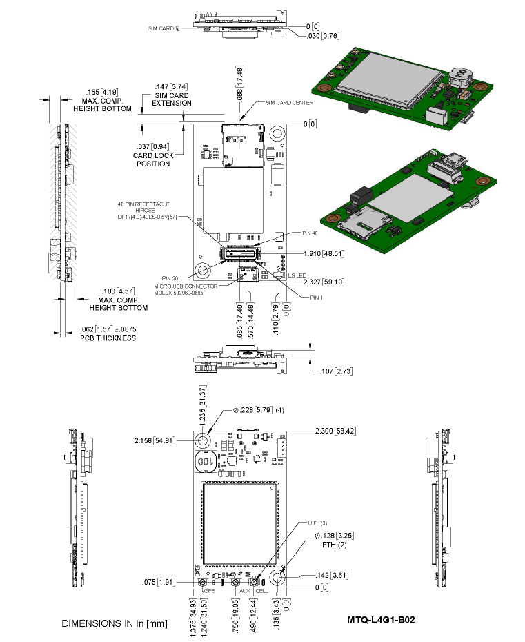
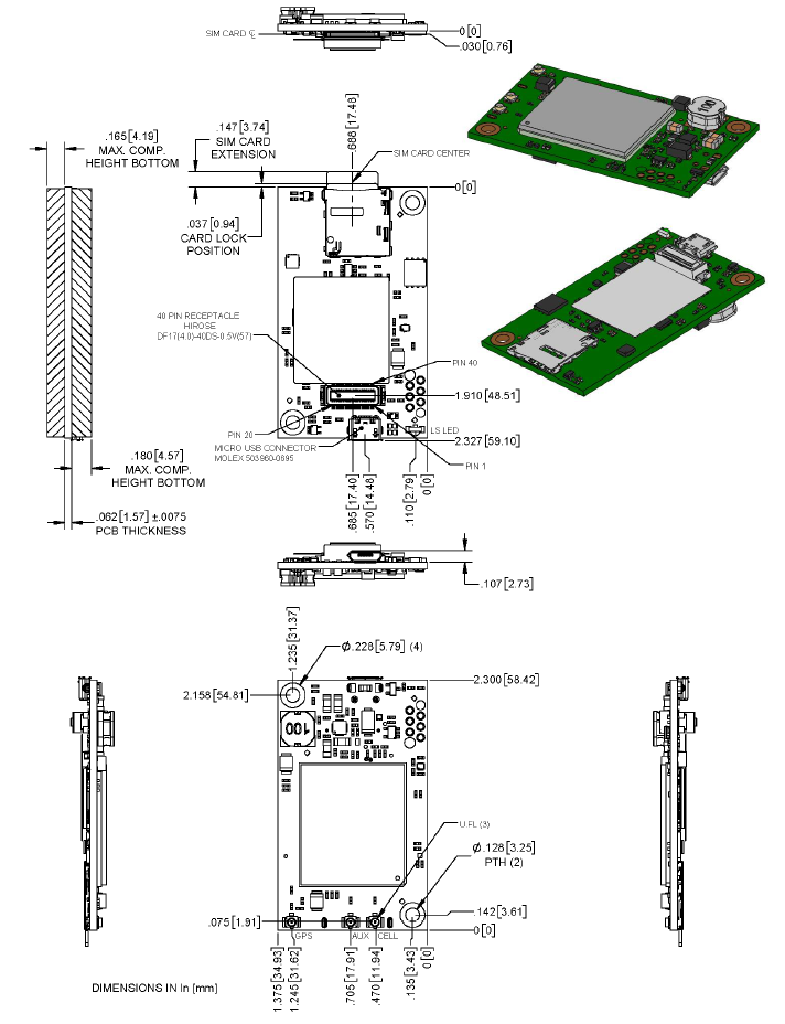
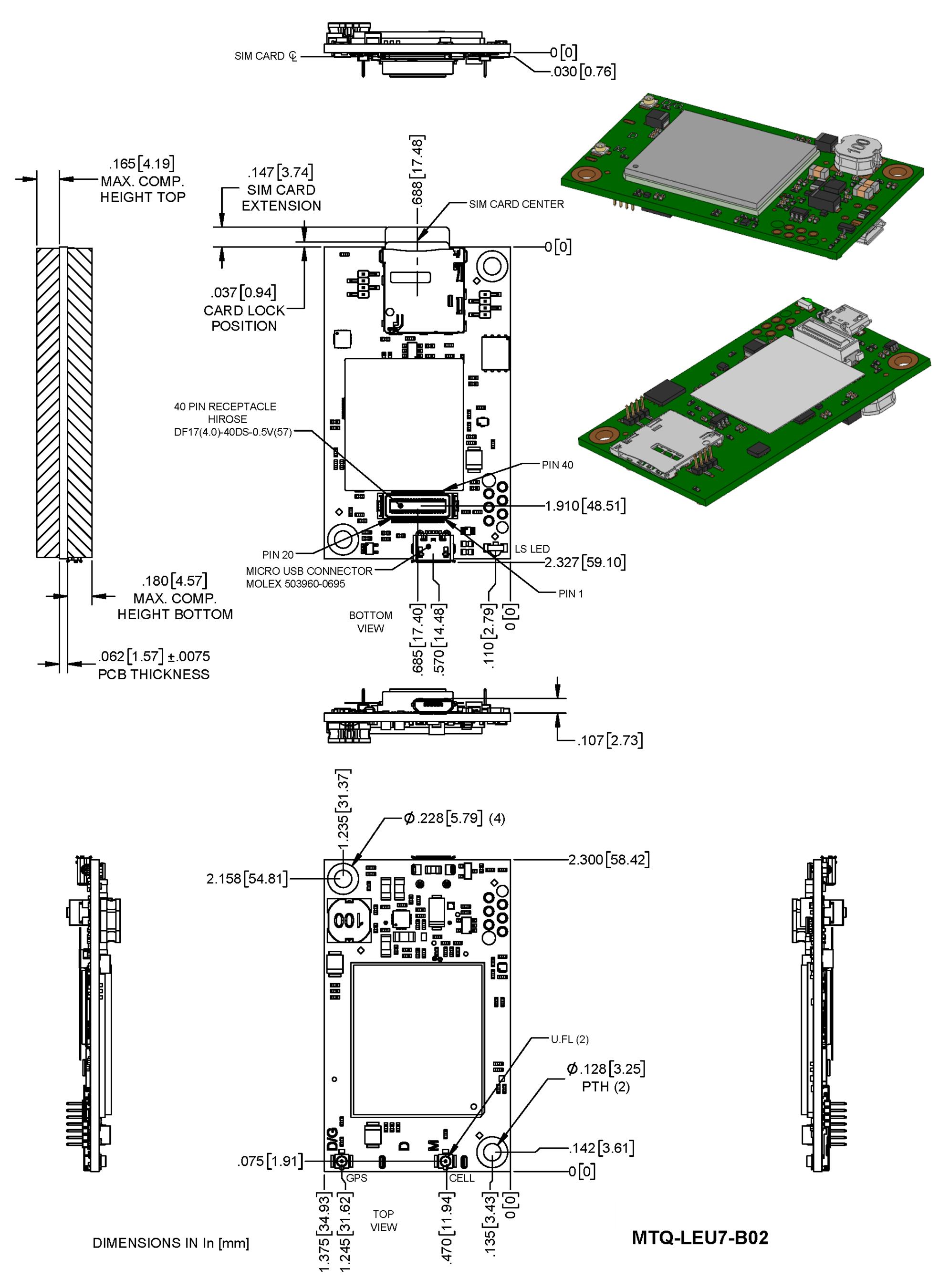
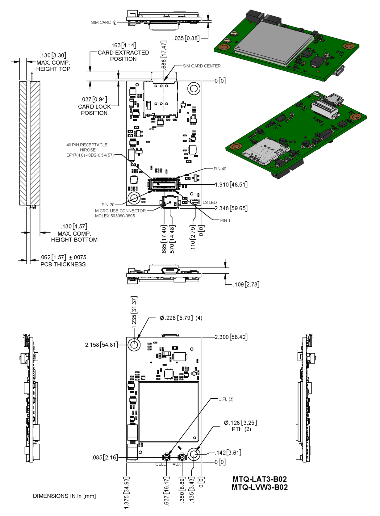
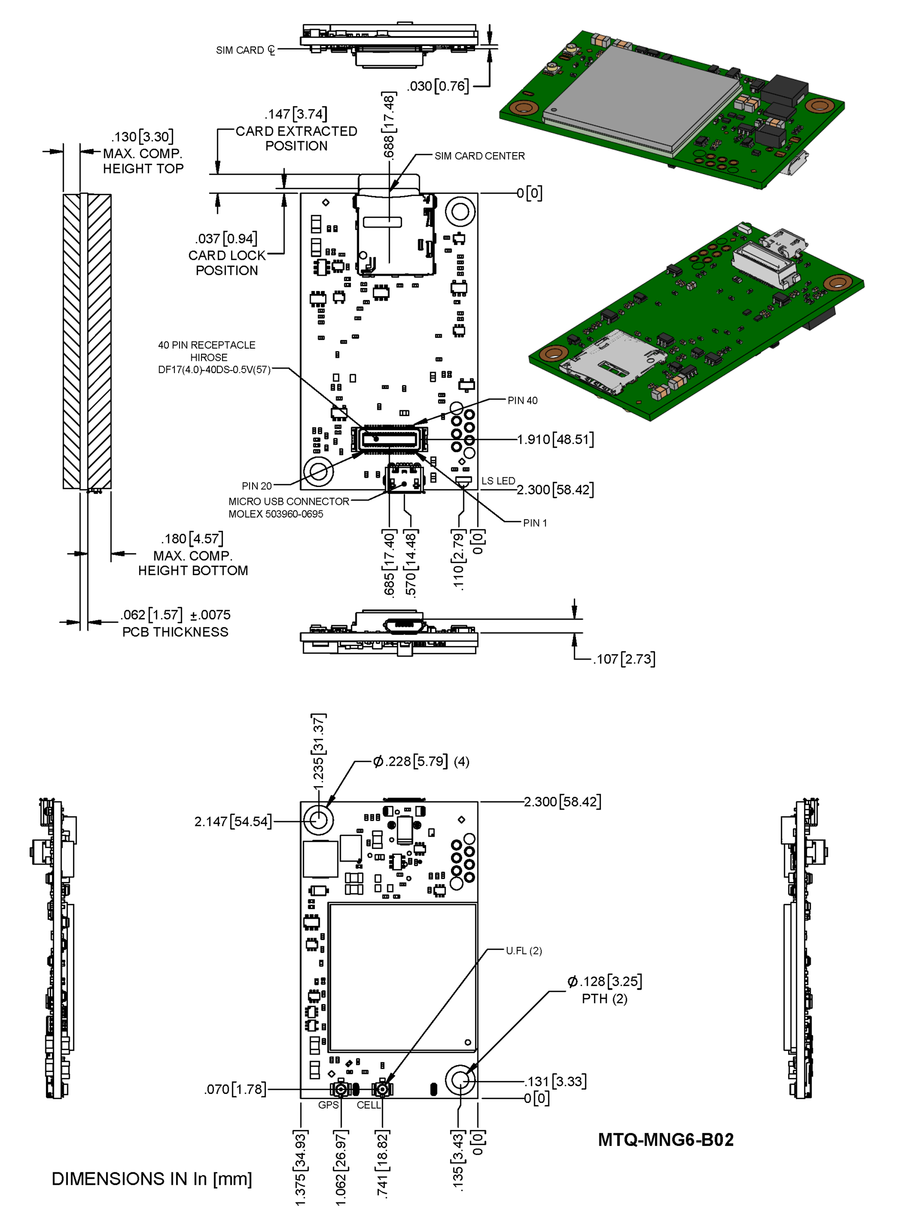
Dimensions
MTQ-L1G2D-B02 Models

MTQ-L4G1-B02 Models
MTQ-LNA7-B02 Models
MTQ-LEU7-B02 Models
MTQ-LAT3 Models
Processor Model (-B01)
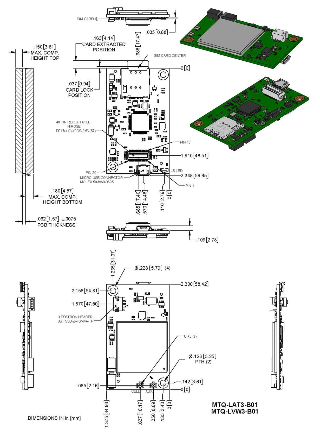
No Processor Model (-B02)
MTQ-MNG6 Models
Descriptions of LEDs
The Link Status LED is located on the SIM side of the device to the right of the Micro USB Connector in the lower right corner.
| LED Indicators | |
|---|---|
| LS | Link Status
|
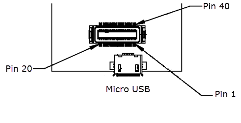
40-Pin Connector Definitions
MTQ-L1G2D-B02
Pin Minimum and Maximum Voltage
| Minimum High Voltage | Maximum Low Voltage | Maximum Input | |
|---|---|---|---|
| Serial Input Signals | 2.0V | 0.8V | 6.5V |
| Serial Output Signals | 2.4V | 0.55 | -- |
![]()
![]()
Pin Definitions
| Pin | Signal Name | Logic Level Voltage1 | Max Voltage | In/Out | Description |
|---|---|---|---|---|---|
| 1 | N/C | ||||
| 2 | N/C | ||||
| 3 | N/C | ||||
| 4 | N/C | ||||
| 5 | GND | GND | GND | Ground Connection | |
| 6 | USB-DATA+ | See USB 2.0 Spec for levels | 3.6V | I/O | USB Data+ connection to cellular module |
| 7 | USB-DATA- | USB Data- connection to cellular module | |||
| 8 | VCC-IN | 3.3 VDC or 5.0 VDC (+/− 5%) | 5.25V | Power Input | Main Power |
| 9 | RADIO_RXD | 0 - 3V | O | Cellular Radio UART Data Output | |
| 10 | RADIO_DCD | 0 - 3V | O | Cellular Radio UART Data Carrier Detect | |
| 11 | RADIO_RI | 0 - 3V | O | Cellular Radio UART Ring indicator | |
| 12 | RADIO_CTS | 0 - 3V | O | Cellular Radio UART Clear to Send (flow control) | |
| 13 | GND | GND | GND | Ground Connection | |
| 14 | SPI_MOSI1 | 0 - 3V | 3.3V | O | Cellular Radio MOSI. |
| 15 | SPI_SCLK1 | 0 - 3V | 3.3V | I | SPI clock. |
| 16 | N/C | ||||
| 17 | N/C | ||||
| 18 | N/C | ||||
| 19 | N/C | ||||
| 20 | N/C | ||||
| 21 | N/C | ||||
| 22 | N/C | ||||
| 23 | N/C | ||||
| 24 | N/C | ||||
| 25 | SPI_SRDY1 | 0 - 3V | O | Cellular Radio SPI Ready. Open drain outputs with 47K pull up to 3V. | |
| 26 | SPI_MISO1 | 0 - 3V | O | Cellular Radio MISO. Open drain outputs with 47K pull up to 3V. | |
| 27 | SPI_CS21 | 0 - 3V | I | Cellular Radio SPI CS. | |
| 28 | GND | GND | GND | Ground Connection | |
| 29 | RADIO_RTS | 0 - 3V | I | Cellular Radio UART Request to Send (flow control) | |
| 30 | RADIO_DSR | 0 - 3V | O | Cellular Radio UART Data Set Ready | |
| 31 | RADIO_DTR | 0 - 3V | I | Cellular Radio UART Data Terminal Ready | |
| 32 | RADIO_TXD | 0 - 3V | I | Cellular Radio UART Serial data input from DTE | |
| 33 | VCC-IN | 3.3 VDC or 5.0 VDC (+/− 5%) | Power Input | Main Power | |
| 34 | LINK_STATUS | 3V | O | Cellular radio link status LED. Open drain outputs with 47K pull up to 3V. | |
| 36 | GND | GND | GND | Ground Connection | |
| 37 | GND | ||||
| 38 | N/C | ||||
| 39 | N/C | ||||
| 40 | N/C |
1SPI pins are for cellular radio, not flash.
MTQ-L4G1-B02
| Pin | Signal Name | Logic Level Voltage1 | Max Voltage | In/Out | Description |
|---|---|---|---|---|---|
| 1 | N/C | ||||
| 2 | N/C | ||||
| 3 | N/C | ||||
| 4 | N/C | ||||
| 5 | GND | GND | GND | Ground | |
| 6 | USB-DATA+ | 0 - 3V 2 | 5.5V | I/O | USB Data |
| 7 | USB-DATA- | ||||
| 8 | VCC-IN | 3.3 - 5V +/-5% | Power Input | Main Power | |
| 9 | RADIO_RXD | 0 - 3V | 3.3V | O | Serial data output to DTE |
| 10 | RADIO_DCD | 0 - 3V | 3.3V | O | Data carrier detect |
| 11 | RADIO_RI | 0 - 3V | 3.3V | O | Ring indicator |
| 12 | RADIO_CTS | 0 - 3V | 3.3V | O | Clear to send (flow control) |
| 13 | GND | GND | GND | Ground | |
| 14 | N/C | ||||
| 15 | N/C | ||||
| 16 | N/C | ||||
| 17 | N/C | ||||
| 18 | N/C | ||||
| 19 | N/C | ||||
| 20 | N/C | ||||
| 21 | N/C | ||||
| 22 | N/C | ||||
| 23 | N/C | ||||
| 24 | N/C | ||||
| 25 | N/C | ||||
| 26 | N/C | ||||
| 27 | RADIO_VDD | 0-1.8V | 1.8V | O | This output is generated by the radio. |
| 28 | GND | GND | GND | Ground | |
| 29 | RADIO_RTS | 0 - 3.3V | 3.3V | I | Request to send (flow control) |
| 30 | RADIO_DSR | 0 - 3V | 3.3V | O | Data set ready |
| 31 | RADIO_DTR | 0 - 3.3V | 3.3V | I | DTE ready |
| 32 | RADIO_TXD | 0 - 3.3V | 3.3V | I | Serial data input from DTE |
| 33 | VCC-IN | 3.3 - 5V +/-5% | Power Input | Main Power | |
| 34 | LINK_STATUS | 3V | O | Radio link status LED | |
| 35 | RESET | 0 - 1.8V | I | Radio reset, treat as open drain, active low | |
| 36 | GND | GND | GND | Ground | |
| 37 | GND | ||||
| 38 | N/C | ||||
| 39 | N/C | ||||
| 40 | N/C |
1A hyphen (-) indicates a range of acceptable logic levels.
2USB D+D-: 5V tolerant inputs / 3V drive-level output
MTQ-LNA7-B02
| Pin | Signal Name | Logic Level Voltage1 | Max Voltage | In/Out | Description |
|---|---|---|---|---|---|
| 1 | N/C | ||||
| 2 | N/C | ||||
| 3 | N/C | ||||
| 4 | N/C | ||||
| 5 | GND | GND | GND | Ground | |
| 6 | USB-DATA+ | 0 - 3V 2 | 5.5V | I/O | USB Data |
| 7 | USB-DATA- | ||||
| 8 | VCC-IN | 3.3 - 5V +/-5% | Power Input | Main Power | |
| 9 | RADIO_RXD | 0 - 3V | 3.3V | O | |
| 10 | RADIO_DCD | 0 - 3V | 3.3V | O | Data carrier detect |
| 11 | RADIO_RI | 0 - 3V | 3.3V | O | Ring indicator |
| 12 | RADIO_CTS | 0 - 3V | 3.3V | O | Clear to send (flow control) |
| 13 | GND | GND | GND | Ground | |
| 14 | N/C | ||||
| 15 | N/C | ||||
| 16 | N/C | ||||
| 17 | N/C | ||||
| 18 | N/C | ||||
| 19 | N/C | ||||
| 20 | N/C | ||||
| 21 | N/C | ||||
| 22 | N/C | ||||
| 23 | N/C | ||||
| 24 | N/C | ||||
| 25 | N/C | ||||
| 26 | N/C | ||||
| 27 | RADIO_VDD | 0-1.8V | 1.8V | O | This output is generated by the radio. |
| 28 | GND | GND | GND | Ground | |
| 29 | RADIO_RTS | 0 - 3.3V | 3.3V | I | Request to send (flow control) |
| 30 | RADIO_DSR | 0 - 3V | 3.3V | O | Data set ready |
| 31 | RADIO_DTR | 0 - 3.3V | 3.3V | I | DTE ready |
| 32 | RADIO_TXD | 0 - 3.3V | 3.3V | I | Serial data input from DTE |
| 33 | VCC-IN | 3.3 - 5V +/-5% | Power Input | Main Power | |
| 34 | LINK_STATUS | 3V | O | Radio link status LED | |
| 35 | RESET | 0 - 1.8V | I | Radio reset, treat as open drain, active low | |
| 36 | GND | GND | GND | Ground | |
| 37 | GND | ||||
| 38 | N/C | ||||
| 39 | N/C | ||||
| 40 | N/C |
1A hyphen (-) indicates a range of acceptable logic levels.
2USB D+D-: 5V tolerant inputs / 3V drive-level output
MTQ-LEU7-B02
| Pin | Signal Name | Logic Level Voltage1 | Max Voltage | In/Out | Description |
|---|---|---|---|---|---|
| 1 | N/C | ||||
| 2 | N/C | ||||
| 3 | N/C | ||||
| 4 | N/C | ||||
| 5 | GND | GND | GND | Ground | |
| 6 | USB-DATA+ | 0 - 3V 2 | 5.5V | I/O | USB Data |
| 7 | USB-DATA- | ||||
| 8 | VCC-IN | 3.3 - 5V +/-5% | Power Input | Main Power | |
| 9 | RADIO_RXD | 0 - 3V | 3.3V | O | |
| 10 | RADIO_DCD | 0 - 3V | 3.3V | O | Data carrier detect |
| 11 | RADIO_RI | 0 - 3V | 3.3V | O | Ring indicator |
| 12 | RADIO_CTS | 0 - 3V | 3.3V | O | Clear to send (flow control) |
| 13 | GND | GND | GND | Ground | |
| 14 | N/C | ||||
| 15 | N/C | ||||
| 16 | N/C | ||||
| 17 | N/C | ||||
| 18 | N/C | ||||
| 19 | N/C | ||||
| 20 | N/C | ||||
| 21 | N/C | ||||
| 22 | N/C | ||||
| 23 | N/C | ||||
| 24 | N/C | ||||
| 25 | N/C | ||||
| 26 | N/C | ||||
| 27 | RADIO_VDD | 0-1.8V | 1.8V | O | This output is generated by the radio. |
| 28 | GND | GND | GND | Ground | |
| 29 | RADIO_RTS | 0 - 3.3V | 3.3V | I | Request to send (flow control) |
| 30 | RADIO_DSR | 0 - 3V | 3.3V | O | Data set ready |
| 31 | RADIO_DTR | 0 - 3.3V | 3.3V | I | DTE ready |
| 32 | RADIO_TXD | 0 - 3.3V | 3.3V | I | Serial data input from DTE |
| 33 | VCC-IN | 3.3 - 5V +/-5% | Power Input | Main Power | |
| 34 | LINK_STATUS | 3V | O | Radio link status LED | |
| 35 | RESET | 0 - 1.8V | I | Radio reset, treat as open drain, active low | |
| 36 | GND | GND | GND | Ground | |
| 37 | GND | ||||
| 38 | N/C | ||||
| 39 | N/C | ||||
| 40 | N/C |
1A hyphen (-) indicates a range of acceptable logic levels.
2USB D+D-: 5V tolerant inputs / 3V drive-level output
MTQ‑LAT3‑B01
| Pin | Signal Name | Logic Level Voltage1 | In/Out | Description |
|---|---|---|---|---|
| 1 | DBX_TX | 3V | O | ST Micro UART debug Tx output |
| 2 | SWCLK | 3V | I | See ST Microcontroller Guide |
| 3 | CHARGE_MON | 0 - VCC‑IN | O | Open‑drain charging status indication output |
| 4 | PWR_GOOD | 0 - VCC‑IN | O | Open‑drain power good status indication output |
| 5 | GND | GND | GND | Ground |
| 6 | USB‑DATA+ | 0 - 3V2 | ||
| 7 | USB‑DATA− | |||
| 8 | VCC‑IN | 3.3 VDC or 5.0 VDC +/− 5% | Power Input | Main Power |
| 9 | IO_00 | I = 0 - 7V, O = 0 - 3V | I/O | General Purpose I/O from ST Microcontroller (STM 32F411) |
| 10 | IO_01 | |||
| 11 | IO_02 | |||
| 12 | IO_03 | |||
| 13 | GND | GND | GND | Ground |
| 14 | IO_04 | I = 0 - 7V, O = 0 - 3V | I/O | General Purpose I/O from ST Microcontroller (STM 32F411) |
| 15 | IO_05 | |||
| 16 | IO_06 | |||
| 17 | IO_07 | |||
| 18 | IO_08 | |||
| 19 | IO_09 | |||
| 20 | IO_10 | |||
| 21 | IO_11 | |||
| 22 | IO_12 | |||
| 23 | IO_13 | |||
| 24 | IO_14 | |||
| 25 | IO_15 | |||
| 26 | IO_16 | |||
| 27 | IO_17 | |||
| 28 | GND | GND | GND | Ground |
| 29 | IO_18 | I = 0 - 7V, O = 0 - 3V | I/O | General Purpose I/O from ST Microcontroller (STM 32F411) |
| 30 | IO_19 | |||
| 31 | IO_20 | |||
| 32 | IO_21 | |||
| 33 | VCC‑IN | 3.3 VDC or 5.0 VDC +/− 5% | Power Input | Main Power |
| 34 | LINK_STATUS | 3V | O | Radio link status LED |
| 35 | RESET | 0 - 5V | I | NRST pin of ST micro, treat as open drain, active low |
| 36 | GND | GND | GND | Ground |
| 37 | GND | |||
| 38 | SWO | 3V | O | See ST Microcontroller Guide |
| 39 | SWDIO | 3V | I | |
| 40 | DBG_RX | 3V | I | ST Micro UART debug Tx input |
1 A hyphen (-) indicates a range of acceptable logic levels.
2 USB D+D−: 5V tolerant inputs / 3V drive‑level output
MTQ‑LAT3‑B02
| Pin | Signal Name | Logic Level Voltage1 | Max Voltage | In/Out | Description |
|---|---|---|---|---|---|
| 1 | N/C | ||||
| 2 | N/C | ||||
| 3 | N/C | ||||
| 4 | PWR_GOOD | 0 - VCC‑IN | O | Open‑drain power good status indication output | |
| 5 | GND | GND | GND | Ground | |
| 6 | USB‑DATA+ | 0 - 3V | 5.5V | I/O | USB Data |
| 7 | USB‑DATA− | ||||
| 8 | VCC-IN | 3.3 VDC or 5.0 VDC +/− 5% | Power Input | Main Power | |
| 9 | RADIO_RXD | 0 - 3V | 3.3V | O | |
| 10 | RADIO_DCD | 0 - 3V | 3.3V | O | Data carrier detect |
| 11 | RADIO_RI | 0 - 3V | 3.3V | O | Ring indicator |
| 12 | RADIO_CTS | 0 - 3V | 3.3V | O | Clear to send (flow control) |
| 13 | GND | GND | GND | Ground | |
| 14 | SPI_MOSI1 | 0 - 3V | 3.3V | O | |
| 15 | SPI_SCLK1 | 0 - 3.3V | 3.3V | I | SPI clock |
| 16 | SPI_CS11 | 0 - 3.3V | 3.3V | I | Serial flash SPI CS |
| 17 | N/C | ||||
| 18 | N/C | ||||
| 19 | N/C | ||||
| 20 | N/C | ||||
| 21 | N/C | ||||
| 22 | N/C | ||||
| 23 | N/C | ||||
| 24 | N/C | ||||
| 25 | SPI_SRDY | I = 0 - 3.3V, O = 0 - 3V | 3.3V | I/O | SPI Ready |
| 26 | SPI_MISO | 0 - 3.3V | 3.3V | I | |
| 27 | SPI_CS21 | 0 - 3.3V | 3.3V | I | Radio SPI CS |
| 28 | GND | GND | GND | Ground | |
| 29 | RADIO_RTS | 0 - 3.3V | 3.3V | I | Request to send (flow control) |
| 30 | RADIO_DSR | 0 - 3V | 3.3V | O | Data set ready |
| 31 | RADIO_DTR | 0 - 3.3V | 3.3V | I | DTE ready |
| 32 | RADIO_TXD | 0 - 3.3V | 3.3V | I | Serial data input from DTE |
| 33 | VCC-IN | 3.3 VDC or 5.0 VDC +/− 5% | Power Input | Main Power | |
| 34 | LINK_STATUS | 3V | O | Radio link status LED | |
| 35 | RESET | 0 - 5V | I | Radio reset, treat as open drain, active low | |
| 36 | GND | GND | GND | Ground | |
| 37 | GND | ||||
| 38 | N/C | ||||
| 39 | N/C | ||||
| 40 | N/C |
1For ‑B02 models only: Pins 14, 15, 16, and 27 are part of the SPI interface. These pins are inputs. If you do not use them, connect them externally to a high‑level signal (preferably through a high pull‑up resistor) to keep them from floating.
MTQ-MNG6-B02
Pin Minimum and Maximum Voltage
| Minimum High Voltage | Maximum Low Voltage | Maximum Input | |
|---|---|---|---|
| Serial Input Signals | 2.0V | 0.8V | 6.5V |
| Serial Output Signals | 2.4V | 0.55 | -- |
Pin Definitions
| Pin | Signal Name | Logic Level Voltage1 | Max Voltage | In/Out | Description |
|---|---|---|---|---|---|
| 1 | NC | ||||
| 2 | NC | ||||
| 3 | NC | ||||
| 4 | NC | ||||
| 5 | GND | GND | GND | Ground Connection | |
| 6 | USB-DATA+ | See USB 2.0 Spec for levels | 3.6V | I/O | USB Data+ connection to cellular module |
| 7 | USB-DATA- | USB Data- connection to cellular module | |||
| 8 | VCC-IN | 3.3 VDC or 5.0 VDC +/− 5% | 5.25V | Power Input | Main Power |
| 9 | RADIO_RXD | 0 - 3V | O | Cellular Radio UART Data Output | |
| 10 | RADIO_DCD | 0 - 3V | O | Cellular Radio UART Data Carrier Detect | |
| 11 | RADIO_RI | 0 - 3V | O | Cellular Radio UART Ring indicator | |
| 12 | RADIO_CTS | 0 - 3V | O | Cellular Radio UART Clear to Send (flow control) | |
| 13 | GND | GND | GND | Ground Connection | |
| 14 | NC | ||||
| 15 | NC | ||||
| 16 | NC | ||||
| 17 | NC | ||||
| 18 | NC | ||||
| 19 | NC | ||||
| 20 | NC | ||||
| 21 | NC | ||||
| 22 | NC | ||||
| 23 | NC | ||||
| 24 | NC | ||||
| 25 | NC | ||||
| 26 | NC | ||||
| 27 | NC | C | |||
| 28 | GND | GND | GND | Ground Connection | |
| 29 | RADIO_RTS | 0 - 3V | I | Cellular Radio UART Request to Send (flow control) | |
| 30 | RADIO_DSR | 0 - 3V | O | Cellular Radio UART Data Set Ready | |
| 31 | RADIO_DTR | 0 - 3V | I | Cellular Radio UART Data Terminal Ready | |
| 32 | RADIO_TXD | 0 - 3V | I | Cellular Radio UART Serial data input from DTE | |
| 33 | VCC-IN | 3.3 VDC or 5.0 VDC +/− 5% | Power Input | Main Power | |
| 34 | LINK_STATUS | 3V | O | Cellular radio link status LED. Open drain outputs with 47K pull up to 3V. | |
| 36 | GND | GND | GND | Ground Connection | |
| 37 | GND | ||||
| 38 | NC | ||||
| 39 | NC | ||||
| 40 | NC |
40‑Pin Connector
|
Use with:
|
Processor Pin Information (B01 models only)
The following table lists the processor pins and how the MTQ uses them.
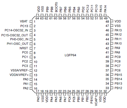
| Net Name | Number | Pin Name | Details |
|---|---|---|---|
| VDD3_3 | 1 | VBAT | Power |
| 3G_ONOFF | 2 | PC13 | Enable line to the Radio |
| 32K_XTAL_ | 3 | PC14 | RTC Clock |
| 32K_XTAL | 4 | PC15 | RTC Clock |
| 26MHZ_CLK_IN | 5 | PH0-OSC_IN | Main Clock |
| 26MHZ_CLK_DRIVE | 6 | PH1-OSC_OUT | Main Clock |
| N_RESET | 7 | NRST | External Reset in |
| IO_10 | 8 | PC0 | GPIO/Analog capable pin |
| IO_11 | 9 | PC1 | GPIO/Analog capable pin |
| IO_8 | 10 | PC2 | GPIO |
| RADIO_PWR | 11 | PC3 | Voltage enable for Telit |
| GND | 12 | VSSA | Power |
| VDD3_3 | 13 | VDDA | Power |
| IO_18/RTS | 14 | PA0 | GPIO/Analog capable pin/USART2_CTS |
| IO_03/CTS | 15 | PA1 | GPIO/Analog capable pin/USART2_RTS |
| IO_00/RXD | 16 | PA2 | GPIO/USART2_TX |
| IO_21/TXD | 17 | PA3 | GPIO/USART2_RX |
| GND | 18 | VSS_4 | Power |
| VDD3_3 | 19 | VDD_4 | Power |
| SPI-SS1 | 20 | PA4 | SPI1 SelectConnects to serial flash pin 1 |
| IO_05/SCK | 21 | PA5 | SPI1 Clock/GPIO |
| IO_16/MISO/SDIO_CMD | 22 | PA6 | SPI1 MSIO/SDIO_CMD /GPIO |
| IO_01/DCD | 23 | PA7 | GPIO |
| IO_12 | 24 | PC4 | GPIO/Analog capable pin |
| VDD1_8_MON | 25 | PC5 | Power |
| IO_9 | 26 | PB0 | GPIO/Analog capable pin |
| IO_02/RI | 27 | PB1 | GPIO |
| BOOT1/BC_NCE | 28 | PB2 | Battery charge enabled. Pulled down by default. |
| RADIO_RTS | 29 | PB10 | Serial comm with the radio |
| VCAP | 30 | PB11/VCAP_1 | Power |
| N16612690 | 31 | VCAP_1/VSS | Power |
| VDD3_3 | 32 | VDD_1 | Power |
| RADIO_CTS | 33 | PB12 | Serial comm with the radio |
| IO_13 | 34 | PB13 | GPIO |
| SPI-SS2 | 35 | PB14 | GPIO for use with external SPI |
| IO_7 | 36 | PB15 | GPIO/SDIO_CK |
| RADIO_TXD | 37 | PC6 | Serial comm with the radio |
| RADIO_RXD | 38 | PC7 | Serial comm with the radio |
| IO_17/SS2/SDIO_D0 | 39 | PC8 | GPIO/SDIO_D0 |
| IO_14/SDIO_D1 | 40 | PC9 | GPIO/SDIO_D1 |
| IO_20/DTR | 41 | PA8 | GPIO |
| IO_19/DSR | 42 | PA9 | GPIO/SDIO_D2 |
| USB_DIR/VBUS | 43 | A10 | USB Switch control, 0=Telit, 1=STM1=STM32F413 |
| FS_DM | 44 | PA11 | USB |
| FS_DP | 45 | PA12 | USB |
| J_TMS /SWDIO | 46 | PA13 | JTAG |
| 47 | VCAP_2/VSS | Power | |
| VDD3_3 | 48 | VDD_2 | Power |
| J_TCK/SWCLK | 49 | PA14 | JTAG |
| J_TDI/C_MON | 50 | PA15 | JTAG |
| SPI-SCK | 51 | PC10 | EPROM/SPI3_SCKConnects to serial flash pin 6. Connects to Telit radio pin F15. |
| SPI-MISO | 52 | PC11 | EPROM/SPI3_MISOConnects to serial flash pin 2. Connects to Telit radio pin D15. |
| SPI-MOSI | 53 | PC12 | EPROM/SPI3_MOSIConnects to serial flash pin 5. Connects to Telit radio pin E15. |
| SPI-SRDY | 54 | PD2 | EPROM/SPI3_SRDYConnects to Telit radio pin J15. |
| J_TDO/SWO | 55 | PB3 | JTAG |
| J_RST/P_GOOD | 56 | PB4 | JTAG |
| IO_4/MOSI/SDIO_D3 | 57 | PB5 | GPIO/SPI1_MOSI/SDIO_D3 |
| DBG_TX | 58 | PB6 | JTAG |
| DBG_RX | 59 | PB7 | JTAG |
| BOOT | 60 | BOOT0 | Reserved. |
| IO_6/SCL/SS1 | 61 | B8 | GPIO/I2C1_SCL |
| IO_15/SDA/SRDY | 62 | PB9 | GPIO/I2C1_SDA |
| GND | 63 | VSS_3 | Power |
| VDD3_3 | 64 | VDD_3 | Power |
Serial Flash Embedded Memory
The M25P16 is a 16Mb (2Mb x 8) serial flash memory device with write protection mechanisms accessed by a SPI-compatible bus.
The serial flash is accessible via the processor pinout on B01 devices. Features include:
- 75 MHz clock frequency (maximum)
- Page program (up to 256 bytes) in 0.64ms (TYP)
- Erase capability
- Sector erase: 512Kb in 0.6 s (TYP)
- Bulk erase: 16Mb in 13 s (TYP)
- Write protection
- Hardware write protection (protected area size defined by non-volatile bits BP0, BP1, BP2)
- Deep power down: 1µA (TYP)
- Electronic signature
- JEDEC standard 2-byte signature (2015h)
- Unique ID code (UID) and 16 bytes of read-only data available upon customer request
- RES command, one-byte signature (14h) for backward compatibility
- More than 100,000 write cycles per sector
- More than 20 years of data retention
This product uses the GigaDevice GD25Q16C serial flash memory device.
For information on features, refer to the serial flash datasheet: https://www.gigadevice.com/flash-memory/gd25q16c
For information on processor connections to serial flash, refer to the table in Processor Pin Information.
Electrical Characteristics
Operating Conditions
| Parameter | Minimum Volts | Maximum Volts |
|---|---|---|
| Supply Range - Vcc | 3.3 VDC +/− 5% | 5.0 VDC +/− 5% |
Absolute Maximum Rating
| Parameter | Minimum Volts | Maximum Volts |
|---|---|---|
| Voltage at any signal pin | −0.3 | 5.5 |
DC Electrical Characteristics
| Parameter | Conditions | Minimum Volts | Maximum Volts |
|---|---|---|---|
| Digital signal input low level | CMOS port IIO=+8 mA |
−0.3 | 0.9 |
| Digital signal input high level | CMOS port IIO=+8 mA |
2.1 | 5.5 |
| Output low level voltage for an I/O pin | CMOS port IIO=+8 mA |
- | 0.4 |
| Output high level voltage for an I/O pin | VDD−0.4 | - | |
| Output low level voltage for an I/O pin | TTL port IIO=+8 mA |
- | 0.4 |
| Output high level voltage for an I/O pin | 2.4 | - | |
| Output low level voltage for an I/O pin | IIO=+20 mA | - | 1.3(1) |
| Output high level voltage for an I/O pin | VDD−1.3(1) | - | |
| Output low level voltage for an I/O pin | IIO=+6 mA | - | 0.4(1) |
| Output high level voltage for an I/O pin | VDD−0.4(1) | - | |
| Output low level voltage for an I/O pin | IIO=+4 mA | - | 0.4(2) |
| Output high level voltage for an I/O pin | VDD−0.4(2) | - | |
| RESET (low active) input low | CMOS port IIO=+8 mA |
- | 0.99 |
| RESET (low active) input high | CMOS port IIO=+8 mA |
LAT3 only = 5.00 Other models = 2.31 |
- |
(1) Guaranteed by characterization results, not tested in production.
(2) Guaranteed by design, not tested in production.
Input/Output Current Ratings
| Output current draw PWR_GOOD, CHG_MON | 5 mA |
| Output current draw all other output pins | 25 mA |
Power Draw
Power Draw - MTQ-L1G2D-B02
Multi-Tech Systems, Inc. recommends you incorporate a 10% buffer into your power source when determining product load.
| Radio Protocol | AT#SHDN or Radio On/Off Mode Current (If Applicable) | Cellular Connection Idle (No Data) | (AVG) Measured Current at Max Power | TX Pulse (AVG) Amplitude Current for Peak Current for HSDPA/LTE | Total Inrush Charge measured in millicoulombs | Total Inrush Charge DURATION during Power up (INRUSH Duration) |
|---|---|---|---|---|---|---|
| 3.3 VDC with Device on the Developer Board | ||||||
| GSM 850 WS46=12 | 22 mA | 71 mA | 243 mA | 927 mA | 1.10 mC | 675 uS |
| WCMDA WS46=22 | 21 mA | 46 mA | 545 mA | 636 mA | 1.10 mC | 675 uS |
| LTE BAND 7 WS46=28 | 21 mA | 46 mA | 627 mA | 712 mA | 1.10 mC | 675 uS |
| 5.0 VDC with Device on the Developer Board | ||||||
| GSM 850 WS46=12 | 22 mA | 65 mA | 236 mA | 790 mA | .210 mC | 1.38 mS |
| WCMDA WS46=22 | 23 mA | 46 mA | 539 mA | 628 mA | .210 mC | 1.38 mS |
| LTE BAND 7 WS46=28 | 23 mA | 46 mA | 550 mA | 568 mA | .210 mC | 1.38 mS |
| 5.0 VDC with Device USB Only | ||||||
| GSM 850 WS46=12 | 20 mA | 48 mA | 280 mA | 1.10 A | .010 mC | 71.2 uS |
| WCMDA WS46=22 | 20 mA | 48 mA | 706 mA | 780 mA | .010 mC | 71.2 uS |
| LTE BAND 7 WS46=28 | 20 mA | 49 mA | 684 mA | 764 mA | .010 mC | 71.2 uS |
- Maximum Power: The continuous current during maximum data rate with the radio transmitter at maximum power.
- Tx Pulse: The average peak current during a GSM850 transmission burst period or HSDPA/LTE connection. The transmission burst duration for GSM850 can vary, depending on what transmission scheme is being deployed (GPRS Class 8, Class 10, GSM, etc.).
- Inrush Charge: The total inrush charge at power on.
Power Draw - MTQ-L4G1-B02D-B01
| Radio Protocol | Power Down Mode via AT+QPOWD (mA) | Power Down Mode via Reset line (uA) | Live Connection Idle - No Data (mA) | Callbox Connection Idle - No Data (mA) | Average Measured Current at Max Power (mA)1 | TX Pulse2 AVG Amplitude Current for Peak Current for HSDPA/LTE (mA) | Total Inrush Charge3 Measured in Millicoulombs (mC) |
|---|---|---|---|---|---|---|---|
| 5.0 VDC with Unit in Developer Card | |||||||
| GSM850 | 9.2 | 561 | 25 | 27 | 289 | 1,310 | 2.06 |
| WCDMA Band 2 (1854 Mhz) | 9.2 | 561 | 22 | 26 | 459 | 548 | 2.06 |
| LTE Band 8 (897.5 Mhz) | 9.3 | 562 | 27 | 48 | 539 | 632 | 2.06 |
- 1Maximum Power: The continuous current during maximum data rate with the radio transmitter at maximum power.
- 2Tx Pulse: The average peak current during a GSM850 transmission burst period or HSDPA/LTE connection. The transmission burst duration for GSM850 can vary, depending on what transmission scheme is being deployed (GPRS Class 8, Class 10, GSM, etc.).
- 3Inrush Charge: The total inrush charge at power on.
Power Draw - MTQ-LNA7-B02
| Radio Protocol | Power Down Mode (mA) | Live Connection Idle - No Data (mA) | Average Measured Current at Max Power (mA)1 | TX Pulse2 Average Amplitude Current for Peak Current for HSDPA/LTE (mA) | Total Inrush Charge3 Measured in Millicoulombs (mC) |
|---|---|---|---|---|---|
| 5.0 VDC with Unit in Developer Card | |||||
| WCDMA Band 2 (1854 Mhz) | 8.6 | 24 | 567 | 672 | 2.03 |
| LTE Band 4 (1732 Mhz) | 8.6 | 28 | 622 | 712 | 2.03 |
| 5.0 VDC USB Only without Developer Card | |||||
| WCDMA Band 2 (1854 Mhz) | 8.5 | 30 | 536 | 630 | 1.03 |
| LTE Band 4 (1732 Mhz) | 8.5 | 36 | 609 | 712 | 1.03 |
- 1Maximum Power: The continuous current during maximum data rate with the radio transmitter at maximum power.
- 2Tx Pulse: The average peak current during a GSM850 transmission burst period or HSDPA/LTE connection. The transmission burst duration for GSM850 can vary, depending on what transmission scheme is being deployed (GPRS Class 8, Class 10, GSM, etc.).
- 3Inrush Charge: The total inrush charge at power on.
Power Draw - MTQ‑LEU7‑B02
| Radio Protocol | Average Measured Current at Max Power (mA)1 | TX Pulse2 Average Amplitude Current for Peak Current for HSDPA/LTE (mA) | Total Inrush Charge3 Measured in Millicoulombs (mC) |
|---|---|---|---|
| 5.0 VDC with Unit in Developer Card | |||
| EGSM 900 | 365 | 1,430 | .377 |
| WCDMA | 650 | 740 | .377 |
| LTE | 843 | 913 | .377 |
| 5.0 VDC USB Only without Developer Card | |||
| EGSM 900 | 293 | 1,510 | .020 |
| WCDMA | 522 | 556 | .020 |
| LTE | 792 | 812 | .020 |
- 1Maximum Power: The continuous current during maximum data rate with the radio transmitter at maximum power.
- 2Tx Pulse: The average peak current during a GSM850 transmission burst period or HSDPA/LTE connection. The transmission burst duration for GSM850 can vary, depending on what transmission scheme is being deployed (GPRS Class 8, Class 10, GSM, etc.).
- 3Inrush Charge: The total inrush charge at power on.
Power Draw - MTQ-LAT3-B01 (Processor)
| Radio Protocol | Sleep Mode | Cellular Connection Idle (No Data) | (AVG) Measured Current at Max Power1 | TX Pulse2 (AVG) Amplitude Current for Peak Current for HSDPA/LTE) | Total Inrush Charge3 Measured in Millicoulombs |
|---|---|---|---|---|---|
| 5.0 VDC with Unit in Developer Card | |||||
| WCDMA | 5 mA | 56 mA | 655 mA | 748 mA | 3.21 mC |
| LTE | 5 mA | 58 mA | 540 mA | 608 mA | 3.21 mC |
| 5.0 VDC without Unit in Developer Card | |||||
| WCDMA | 5 mA | 62 mA | 715 mA | 808 mA | 3.45 mC |
| LTE | 5 mA | 62 mA | 555 mA | 624 mA | 3.45 mC |
- 1Maximum Power: The continuous current during maximum data rate with the radio transmitter at maximum power.
- 2Tx Pulse: The average peak current during a GSM850 transmission burst period or HSDPA/LTE connection. The transmission burst duration for GSM850 can vary, depending on what transmission scheme is being deployed (GPRS Class 8, Class 10, GSM, etc.).
- 3Inrush Charge: The total inrush charge at power on.
Waveforms
USB only inrush charge of 3.45 mC with 37.2 mS duration
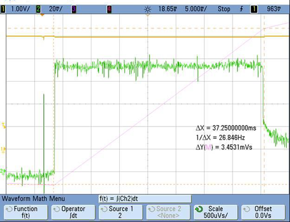
Total Inrush charge of 3.21 mC with 41.1 mS duration
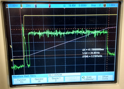
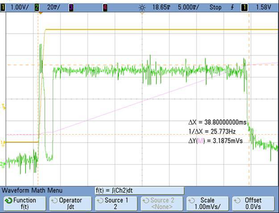
Power Draw - MTQ-LAT3-B02 (No Processor)
| Radio Protocol | Radio On/Off Mode Current (Amps) | Cellular Connection Idle (No Data) | (AVG) Measured Current at Max Power1 | TX Pulse2 (AVG) Amplitude Current for Peak Current for HSDPA/LTE | Total Inrush Charge3 Measured in Millicoulombs |
|---|---|---|---|---|---|
| 5.0 VDC without Unit in Developer Card | |||||
| WCDMA | 25 mA | 37 mA | 590 mA | 660 mA | 3.18 mC |
| LTE | 25 mA | 38 mA | 510 mA | 572 mA | 3.18 mC |
| 5.0 VDC with Unit in Developer Card | |||||
| WCDMA | 25 mA | 43 mA | 640 mA | 700 mA | 3.68 mC |
| LTE | 25 mA | 45 mA | 525 mA | 592 mA | 3.68 mC |
- 1Maximum Power: The continuous current during maximum data rate with the radio transmitter at maximum power.
- 2Tx Pulse: The average peak current during a GSM850 transmission burst period or HSDPA connection. The transmission burst duration for GSM850 can vary, depending on what transmission scheme is being deployed (GPRS Class 8, Class 10, GSM, etc.).
- 3Inrush Charge: The total inrush charge at power on.
Waveforms
Total inrush current of 3.18 mC with 38.8 mS duration
USB only, total inrush current of 3.68 mC with 37.8 mS duration
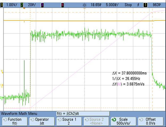
Power Draw - MTQ-MNG6-B02
Multi-Tech Systems, Inc. recommends you incorporate a 10% buffer into your power source when determining product load.
| Radio Protocol | PSM Mode (CPSMS) | eDRX Mode | eDRX Mode with CFUN=5 | Cellular Connection Idle (No Data) (Amps) | Average Measured Current at Max Power | TX Pulse (AVG) Amplitude Current for Peak Current for LTE | Total Inrush Charge measured | Total Inrush Charge DURATION during Power up |
|---|---|---|---|---|---|---|---|---|
| 3.3 VDC with Device on the Developer Board | ||||||||
| GSM 850 UDK Card | N/A | N/A | N/A | 41 mA | 290 mA | 1.9 A | 0.196 mC | 1.38 mS |
| LTE BAND 12 UDK Card 707.5Mhz | 21 mA | 40 mA | N/A | 53 mA | 355 mA | 896 mA | 0.196 mC | 1.38 mS |
| 5.0 VDC with Device on the Developer Board | ||||||||
| GSM 850 UDK Card | N/A | N/A | N/A | 40 mA | 274 mA | 1.78 A | 0.254 mC | 1.35 mS |
| LTE BAND 12 UDK Card 707.5Mhz | 21 mA | 39 mA | N/A | 41 mA | 350 mA | 888 mA | 0.254 mC | 1.35 mS |
| 5.0 VDC with Device USB Only | ||||||||
| GSM850 USB Only | N/A | N/A | N/A | 40 mA | 304 mA | 1.79 A | 0.10 mC | 2.06 mS |
| LTE BAND 12 USB Only 707.5Mhz | 19 mA | 44 mA | N/A | 43 mA | 383mA | 1.1 A | 0.10 mC | 2.06 mS |
- Maximum Power: The continuous current during maximum data rate with the radio transmitter at maximum power.
- Tx Pulse: The average peak current during a GSM850 transmission burst period or LTE connection. The transmission burst duration for GSM850 can vary, depending on what transmission scheme is being deployed (GPRS Class 8, Class 10, GSM, etc.).
- Inrush Charge: The total inrush charge at power on.
Labels
Approvals and Certifications
This device is an industry and/or carrier approved modem. In most cases, when integrated and used with an antenna system that was part of the MultiTech modem certification, additional approvals or certifications are not required for the device that you develop as long as the following requirements are met:
- PTCRB Requirements: The antenna system cannot be altered. The antenna system must be the same type with similar in‐band and out‐of‐band radiation patterns and maintain the same specifications. Refer to the FCC grant information for details.
- Model Identification: The MultiTech model identification allows the carrier to verify the modem as one of its approved models. This information is located on the modem's label below the bar code.
Example Labels
This device complies with part 15 of the FCC Rules. Operation is subject to the following two conditions: (1) This device may not cause harmful interference, and (2) this device must accept any interference received, including interference that may cause undesired operation.
The label shown is not the actual size.
- 1 - MultiTech Model Identification
- 2 - MultiTech Ordering Part Number
- 3 - IMEI
|
Device Label 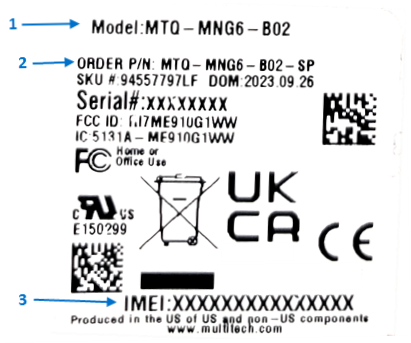 |
Package Label 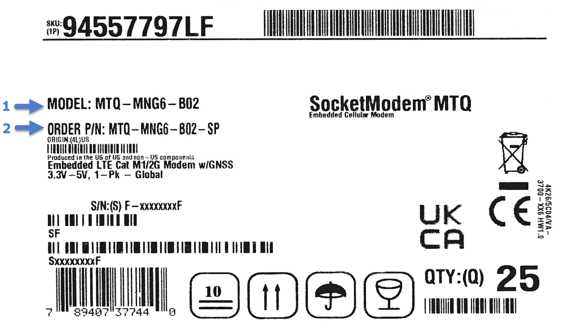 |
Antenna Information
Antenna System Cellular Devices
The cellular/wireless performance depends on the implementation and antenna design. The integration of the antenna system into the product is a critical part of the design process. Therefore, it is essential to consider it early so that the performance is not compromised. Devices were approved with the antenna(s) described below and for alternate antennas meeting the given specifications.
The antenna system is defined as the U.FL connection point from the device to the specified cable specifications and specified antenna specifications.
The antenna system is defined as the SMA connection point from the device to the specified cable specifications and specified antenna specifications.
Antenna
Devices were approved with the following antenna:
| Manufacturer: | Wieson |
| Description: | LTE Antenna with SMA-Male Connector |
| Model Number | GY115IE002-001 |
MultiTech ordering information:
| Model | Quantity |
|---|---|
| ANLTE4-1HRA | 1 |
| ANLTE4-2HRA | 2 |
| ANLTE4-10HRA | 10 |
| ANLTE4-50HRA | 50 |
Antenna Specifications
| Category | Description | |
|---|---|---|
| Frequency Range | 0.698 - 0.96 GHz | |
| 1.710 - 2.170 GHz | ||
| 2.30 - 2.69 GHz | ||
| VSWR | 3:1 maximum | |
| Gain | 2.06 dBi | |
| Impedance | 50Ω nominal | |
| Radiation | Omni-directional | |
| Polarization | Linear, vertical | |
LTE Antenna Information
The cellular radio portion of the device is approved with the following antenna or for alternate antennas meeting the given specifications.
| Manufacturer: | EAD Ltd. |
| Description: | LTE Antenna with SMA-Male Connector |
| Model Number: | WTR7270 |
| MultiTech Part Number: | 45009760L |
MultiTech ordering information:
| Model | Quantity |
|---|---|
| ANLTE3-2HRA | 2 |
| ANLTE3-10HRA | 10 |
| ANLTE3-50HRA | 50 |
Antenna Specifications
| Category | Description | |
|---|---|---|
| Frequency Range | 690-960 MHz | |
| 1710-2700 MHz | ||
| Power Rating | 10 W | |
| VSWR | < 2.0:1 | |
| Gain | 1 dBi | |
| Radiating Element | 1/2 wave element | |
| Polarization | Linear | |
LTE Antenna MISO
LTE devices use Multiple Input and Single output (MISO) to improve the downlink connection (cell tower to mobile). It has no effect on the uplink (mobile to cell tower).
Selecting Antennas
Select an antenna based on your product and application. Typically, both antennas are the same because either can be the main receive antenna. However, if the antenna connectors are too close together, use a similar antenna on a short cable for the second receive only antenna.
Antenna Approvals and Safety Considerations
Note the following:
- The carriers conduct antenna diversity tests.
- There are no EMC concerns about antenna diversity.
- All antennas need to have a minimum flammability rating.
- Safety requirements depend on your final product.
- Antennas are not approved for outdoor use. Do not extend antennas outside of any building.
Power Draw
There are no significant power draw differences.
FCC Requirements
There cannot be any alteration to the authorized antenna system. The antenna system must be the same type with similar in‐band and out‐of‐band radiation patterns and should not exceed the maximum gain information detailed in the FCC Grant.
OEM Integration
FCC & IC Information to Consumers
The user manual for the consumer must contain the statements required by the following FCC and IC regulations: 47 C.F.R. 15.19(a)(3), 15.21, 15.105 and RSS-Gen Issue 3, Dec 2010; 7.1.2 and 7.1.3
FCC Grant Notes
The OEM should follow all the grant notes listed below. Otherwise, further testing and device approvals may be necessary.
FCC Definitions
Portable: (§2.1093) — A portable device is defined as a transmitting device designed to be used so that the radiating structure(s) of the device is/are within 20 centimeters of the body of the user.
Mobile: (§2.1091) — A mobile device is defined as a transmitting device designed to be used in other than fixed locations and to generally be used in such a way that a separation distance of at least 20 centimeters is normally maintained between the transmitter’s radiating structure(s) and the body of the user or nearby persons.
Actual content pending Grant: This device is a mobile device with respect to RF exposure compliance. The antenna(s) used for this transmitter must be installed to provide a separation distance of at least 20 cm from all persons, and must not be collocated or operate in conjunction with any other antenna or transmitter except in accordance with FCC multi-transmitter product guidelines. Installers and end-users must be provided with specific information required to satisfy RF exposure compliance for installations and final host devices. (See note under Grant Limitations.) Compliance of this device in all final host configurations is the responsibility of the Grantee.
Host Labeling
The following statements are required to be on the host label:
- Contains FCC ID: {Add the device FCC ID}
- Contains IC: {Add the device IC ID}
For device specific FCC and IC ID information refer to the FCC and ID grant information topics in the Regulatory Information chapter. For additional labeling requirements and label examples, refer to the Labels chapter.
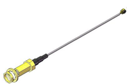
SMA to U.FL Cables
The developer kit includes three 4.5" SMA to U.FL cables which are preinstalled on the developer board. Consult the mechanical drawings for your device to determine which antenna to connect to which U.FL connector on the device.
Connecting an Antenna through the Developer Board Connectors
Depending on the device model, you can either connect antennas directly to the device or through the RSMA-to-U.FL antenna cable on the developer board.
To connect an antenna to the device through the developer board:
- Determine which SMA connector you want to use for the antenna.
- Finger tighten the antenna to the SMA connector.
- Attach the U.FL connector from the cable to the connector on the
device.

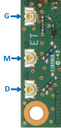
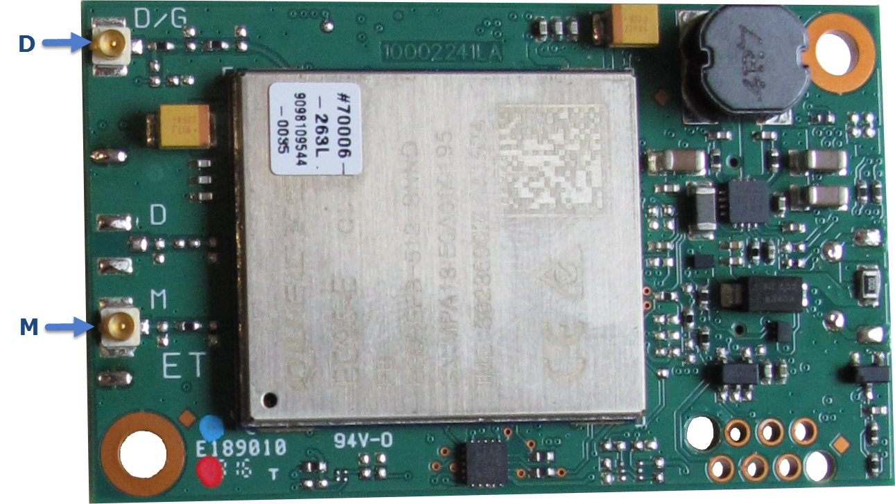
G = GNSS (may not apply to your device)
M = Main
D = Auxiliary/Diversity (may not apply to your device)

Installation
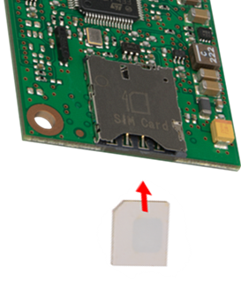
Installing a SIM Card on a SocketModem
When using the SocketModem with a developer board, install the SIM card before mounting the SocketModem on the developer board.
With the contact side facing down, align the notched edge as shown on the SocketModem’s SIM holder and slide the SIM card completely into the SIM holder.
USB Cable Recommendations
To avoid enumeration or power issues if your device has a USB connector:
- Use a high-speed USB cable that is as short as possible.
- Use a well-shielded cable with at least 24 AWG wire pair for power/ground and 28 AWG wire pair for data lines.
- If possible, use a USB port that connects directly to the motherboard rather than a USB port with added cabling inside the computer chassis.
- Use USB 3.0 ports if available. These ports are typically rated for more current.
- The USB cable is available through MultiTech. The part number is CA-USB-A-MINI-B-3CA-USB-A-MICRO-B-3.
Device Drivers
Install drivers on your computer before connecting the device.
The cellular radio's USB device driver is available on your model's page.
- Go to https://multitech.com/all-products/cellular/embedded-modems/multitech-socketmodem-mtq-iot-cellular-embedded-modem-and-system-on-module/https://www.multitech.com/brands/socketmodem-cell and click on your model. Download the driver from Downloads.
- The USB Driver Installation Guide (S000616) is included in the driver download and is also available under Manuals on your model's page.
Operation
Developing with an MTQ in Mbed
Build applications written for the MTQ are built on top of the Arm®Mbed™ library and can include the MTSAS library for easy cellular radio use.
The MTQ ships with AT pass‑through firmware, which directly connects the cellular radio to the external serial port on the MTUDK2‑ST‑CELL developer board. The firmware:
- Runs at 115200 baud by default to match with the cellular radio’s default baud rate.
- Prints debug messages from the debug port at 115200 baud.
- Allows users to increase or decrease the application’s baud rate by entering a plus (+) or minus (−) character on the USB debug port. Issuing a plus or minus character on the USB debug port changes the external serial port speed as well as the speed of the link between the processor and the radio. The speed of the USB debug port on reset is always 115200 to match the radio’s default regardless of the baud rate used at the time of reset.
- Uses RTS/CTS flow control on the serial connection to the radio and on the external serial connection. Enables RTS/CTS flow control on terminal emulators used with the AT pass‑through firmware.
MTSCellularInterface Library
The MTSCellularInterface software library on mbed provides a consistent interface to the cellular radio on each MTQ module. The interface includes:
- TCP sockets
- UDP sockets
- HTTP/HTTPS requests
- SMS messaging
- GPS if supported by the radio
- Access to common radio information like signal strength, registration, etc.
The library provides an easy‑to‑use API for interacting with the cellular radio. It identifies the radio and uses proper AT commands for that radio type, which allows the same application to run on multiple MTQ models with no software changes.
About Mbed™
Arm Mbed is a free, open‑source platform and operating system for embedded devices using the Arm Cortex‑M microcontrollers. The platform includes a standards‑based C/C++ SDK, a microcontroller HDK, and supported development boards, an online compiler and online developer collaboration tools.
Programming the MTQ Microcontroller
With the MTQ and the MTUDK2‑ST‑CELL developer board, use the Arm Mbed ecosystem to program the microcontroller. Compile in the cloud or locally, copy the resulting binary file to the Mbed USB drive, and reset the MTQ.
All MTQ software is open source.
ST Microelectronics STM32F411xC/ESTMicroelectronics STM32F413RH
For information on the STM32F411xC/E microcontroller, refer to:
For information on the STM32F413RH microcontroller, refer to:
Known Issues
The issues below have been identified with this device.
On LVW3 version 20.00.12 and LAT3 version 20.00.522 devices:
- A TCP file transfer in USB mode may drop the socket connection if sending as
little as 60-62 KB of data. If this occurs, then try the following:
- Re-open the socket
- Resend the file
- The AT#SCFG command won't set sockets 4-6 with #sgact=2,1. The following
commands will generate the error +CME ERROR: wrong mode.
- AT#SCFG=4,3,300,240,600,50
- AT#SCFG=5,3,300,240,600,50
- AT#SCFG=6,3,300,240,600,50
On LVW3 version 20.00.12 devices:
- When using AT#PING+, the device will ping, but will not get a response back.
- For example:
- AT#PING="www.google.com",4,32,450
- #PING: 01,"216.58.192.196",600,255
- Warning:(1) IP(216.58.192.196) ReplyTime(600) 100ms Ping Timeout(450) 100ms
- The device will not send an SMS and this message appears: Error! SMS message time out (60) seconds waiting on +CMGS:".
Communications Flow
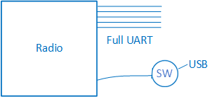
MTQ-L4G1-B02, MTQ-LNA7-B02, and MTQ-LEU7-B02 (No Processor Models)
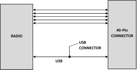
- Simultaneous serial and USB communication are allowed on this device.
MTQ-LAT3-B01 (Processor Model)
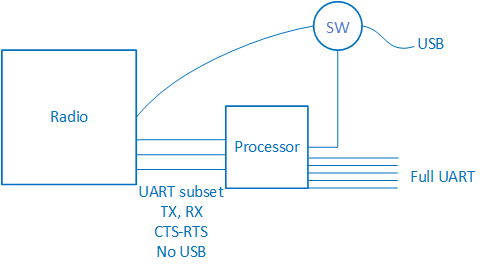
- The B01 has a UART subset as well as GPIO (4 pin UART (tx/rx/rts/cts)
- If needed, use the GPIOs for additional UART signaling.
- The USB port can switch between a connection to the radio or a connection to the processor. The USB selection is controlled via programming on the processor. There is no USB between the radio and the processor.
MTQ-LAT3-B02 (No Processor Model)
MTQ-MNG6-B02 (No Processor Model)
- When the USB interface is used via the 40‑pin connector or the USB connector, the serial interface to the radio will not function.
- Switching between the USB interface and serial port requires a reset. The cellular radio checks for a USB connection upon reset. If USB is not present, it will only use the serial port. If USB is present upon reset, it will only use USB.
Communicating with the Device
Following are three options for communicating with the device.
- Install USB drivers and plug into the micro USB connector. No need for a host board.
- Access the device's USB interface via pins 6 and 7 of the 40-pin connector. Data pins 6 and 7 are in parallel with the micro USB connector on the device. There is no connection to pins 6 and 7 on the developer board.
- Establish serial communication using Multitech developer board MTUDK2. See the Developer Guide, Universal Developer Kit MTUDK2-ST-CELL.R1 (part number S000799) for more information.
Following are three options for communicating with the device.
- Install cellular radio USB drivers and plug into the micro USB connector. No need for a host board.
- Establish serial communication using MultiTech developer board MTUDK2. See the Developer Guide, Universal Developer Kit MTUDK2-ST-CELL.R1 (part number S000799) for more information.
- Install cellular radio USB drivers. Access the device's USB interface via pins 6 and 7 of the 40-pin connector. Data pins 6 and 7 are in parallel with the micro USB connector on the device. There is no connection to pins 6 and 7 on the developer board.
Configuring Device Firmware for Your Cellular Network
Before connecting to a cellular network, you need to configure the device for that cellular network. This step is required only the first time you use the device and if you change cellular carrier.
Carrier Values
- 0 AT&T/other networks
- 1 Verizon
- 2 ROW (Other global).
- 3 Australia
Checking the Cellular Network
To check the device's current cellular network:
AT#FWSWITCH?Setting the Cellular Network
To set the cellular network, issue the following:
AT#FWSWITCH=<carrier value>,1,1,The device automatically reboots twice. After the second reboot, the device is ready for configuring the data connection.
For more information on AT#FWSWITCH, refer to the AT command reference guide.
Examples
AT#FWSWITCH=1,1,1
OK
AT
OK
To switch carrier networks:
From AT&T to Verizon:
AT#FWSWITCH=1,1,1From Verizon to AT&T:
AT#FWSWITCH=0,1,1Configuring a Data Connection
Configure the device before making a cellular data connection. Configuration changes are saved automatically.
Configuring Packet Data Protocol
Use a Packet Data Protocol (PDP) context to configure the device to use your carrier’s packet data services. Multiple PDP contexts are stored in an ordered list. Generally, a carrier approves only one PDP context in the list to configure and use for a data connection with their network.
To view the current PDP context list use the following AT command:
AT+CGDCONT?`Example
AT+CGDCONT?
+CGDCONT: 1,"IPV4V6","","0.0.0.0.0.0.0.0.0.0.0.0.0.0.0.0",0,0,0,0
+CGDCONT: 2,"IPV4V6","vzwadmin","0.0.0.0.0.0.0.0.0.0.0.0.0.0.0.0",0,0,0,0
+CGDCONT: 3,"IPV4V6","vzwinternet","0.0.0.0.0.0.0.0.0.0.0.0.0.0.0.0",0,0,0,0
+CGDCONT: 4,"IPV4V6","vzwapp","0.0.0.0.0.0.0.0.0.0.0.0.0.0.0.0",0,0,0,0
+CGDCONT: 5,"IPV4V6","vzwclass6","0.0.0.0.0.0.0.0.0.0.0.0.0.0.0.0",0,0,0,0
+CGDCONT: 6,"IPV4V6","vzwiotts","0.0.0.0.0.0.0.0.0.0.0.0.0.0.0.0",0,0,0,0

OK`
Before configuring a PDP context use the following to stop the device from automatically connecting to the cellular network and registering:
AT+COPS=2
After configuring the PDP context(s) use the following to resume automatic connection and registration:
AT+COPS=0Configuring APN
The Access Point Name (APN) is a string in the PDP context that defines the network path for cellular data connectivity. The APN must match the carrier’s value provided with the SIM
Configuring Verizon APN
Verizon automatically pushes the necessary PDP context details, including the APN, to the device. If the APN is not pushed automatically, use the following AT commands to set the APN.
AT+COPS=2
AT+CGDCONT=1,"IPV4V6","<APN>"
AT+COPS=0Verizon Example
AT+COPS=2
OK
AT+CGDCONT=1,"IPV4V6","mw01.vzwstatic"
OK
AT+COPS=0
OK
Configuring APN for AT&T and Other Networks
AT&T and other networks may not pushes PDP context details, including the APN, to the device. Use the following AT commands to set the APN.
AT+COPS=2
AT+CGDCONT=1,"IPV4V6","<APN>"
AT+COPS=0AT&T Example
AT+COPS=2
OK
AT+CGDCONT=1,"IPV4V6","broadband"
OK
AT+COPS=0
OK
Registering the Device on a Cellular Network
When configured with AT+COPS=0 the device automatically attempts to register with a carrier network. With the SIM and device properly configured and good reception network registration takes less than a minute. Otherwise, it may take more than 5 minutes.
To determine the device’s registration status, use one of the following three AT commands. If any return n,1 or n,5 then the device registered with the network automatically:
AT+CREG?
AT+CEREG?
AT+CGREG?
Return Values
- n,0 = Time-out or not searching
- n,1 = Registered
- n,2 = Searching
- n,3 = Carrier denied connection (contact carrier for guidance)
- n,5 = Registered, roaming
If the device has not registered with the network, wait a few minutes before issuing one of the AT+C*REG commands again.
Examples
AT+CREG?
+CREG: 0,1

OK
AT+CEREG?
+CEREG: 0,1

OK
AT+CGREG?
+CGREG: 0,1

OK
Testing Cellular Data
Once the device is configured and registered with the cellular network, activate a PDP context and conduct a ping test to ensure the device is sending and receiving data.
Activating a PDP Context
Before sending data, activate a carrier specific PDP context with the following.
AT#SGACT=1,1Example
AT#SGACT=1,1
#SGACT: 100.72.154.34,38.0.16.20.176.134.63.233.0.0.0.0.187.242.184.1

OK
Conducting a Ping Test
After activating the PDP context, use AT#PING to verify network connectivity.
AT#PING="<Domain or IP Address>"
Example:
AT#PING="8.8.8.8"
#PING: 01,"8.8.8.8",0,114
#PING: 02,"8.8.8.8",0,114
#PING: 03,"8.8.8.8",1,114
#PING: 04_Cel,"8.8.8.8",2,114

OK
Configuring Low Power Options
See Power Down the Device for lowest power consumption.
AT+CPSMSAT+CEDRXSAT+CFUNPower Down the Device
To properly power down your L4G1, LNA7, or LEU7 device, use the following sequence:
- Issue the AT+QPOWD command or hold the reset line (pin 35) LOW.
- Wait up to 65 seconds for POWERED DOWN message or until RADIO_VDD (pin 27) goes LOW.
- Remove power to the MTQ.
To properly power down your L1G2D or MNG6 device, use the following sequence:
- Issue the AT+SHDN command or hold the reset line (pin 35) LOW.
- Wait for 30 seconds or until RADIO_VDD (pin 27) goes LOW.
- Remove power to the MTQ.
Device RESET (Pin 35)
The RESET pin takes care of properly powering up and powering down the cellular radio module.
Holding the RESET pin LOW for >50ms initiates a power up or power down sequence, depending on its previous state.
RESET Function on Initial Power Up
- The full power up cycle may take up to 30 seconds before all AT commands are available.
- If the RESET pin is LOW when the radio completes the power up sequence, the radio initiates a power down sequence.
RESET Function when the Radio Module is Powered
- The full power down cycle may take up to 65 seconds, during which time the radio is properly deregistered.
- If the RESET pin is in a continuous LOW state, the radio will stay off.
- You can monitor the state of RADIO_VDD (pin 27); when this pin goes LOW, the radio power is off.
- If the RESET pin is set to HIGH, it will initiate a power up sequence.
Device Reset
MTQ-LAT3-B01 Devices
Reset the Processor
Pin 35 [RESET] on the 40-pin connector is connected to pin 7 [NRST] on the STM32F411RE processor which controls the N_RESET signal for the system.
To reset the processor, apply a reset pulse to N_RESET as follows:
- The minimum recommended reset pulse is 200 μs.
- The maximum reset pulse is 900 ms.
- An unconditional shutdown of the radio
- An uncontrolled disconnection from the network
- The radio to restart which may take 10 seconds or more for it to recover and complete the restart process.
Reset the Radio
Pin 2 [PC13] on the STM32F411RE processor is connected to a tiny9 supervisory processor which controls the 3G_ONOFF signal to the radio.
To reset the radio, drive pin 2 low for:
- A minimum of 50 ms and
- A maximum of 1 second.
Power Down the Radio
MTQ-LAT3-B02 Devices
Pin 35 [RESET] on the 40-pin connector is connected to, and controls, the 3G_ONOFF signal which controls the radio.
MTQ-LAT3-B02 devices may be reset via software or hardware as follows:
Software Reset
To reboot the device, issue an AT#REBOOT command.
To initiate a soft reset, issue an ATZ command.
Hardware Reset
- A minimum of 50 ms and
- A maximum of 1 second.
Sleep Mode
Control radio sleep mode with the GPIO pin PC13 (3G_ONOFF) on the onboard processor. See also 3G_ONOFF Signal.
- Setting PC13 to Low and holding it low turns the radio off, causing it to draw minimal power.
- Setting PC13 to High resets and wakes up the device.
- Refer to +CFUN in the AT Command Reference Guide for other sleep options.
Note: If using +CFUN commands, then reset the device via the PC13 (3G_ONOFF) toggle low to high to bring the radio out of +CFUN sleep mode.
Low Power Options
See Power Down the Device for the lowest power consumption.
- Refer to AT+QSCLK in the AT Command Reference Guide for details on sleep mode and other options.
Firmware Over the Air (FOTA) for Verizon
Also known as Firmware Update Over the Air (FUOTA). At times, your device may require a critical update to radio firmware for devices connecting to the network. To stay compliant to Verizon’s requirements you must implement FOTA. Failure to perform a critical update could result in losing access to the Verizon network. For information and examples go to https://multitech.com/verizon-firmware-over-the-air-fota.
Disposal
Instructions for Disposal of WEEE by Users in the European Union
The symbol shown below is on the product or on its packaging, which indicates that this product must not be disposed of with other waste. Instead, it is the user's responsibility to dispose of their waste equipment by handing it over to a designated collection point for the recycling of waste electrical and electronic equipment. The separate collection and recycling of your waste equipment at the time of disposal will help to conserve natural resources and ensure that it is recycled in a manner that protects human health and the environment. For more information about where you can drop off your waste equipment for recycling, contact your local city office, your household waste disposal service or where you purchased the product.
|
July, 2005 |
Regulatory Information
FCC 47 CFR Part 15 Regulation Class B Devices
This equipment generates, uses, and can radiate radio frequency energy and, if not installed and used in accordance with the instructions, may cause harmful interference to radio communications. However, there is no guarantee that interference will not occur in a particular installation.
If this equipment does cause harmful interference to radio or television reception, which can be determined by turning the equipment off and on, the user is encouraged to try to correct the interference by one or more of the following measures:
- Reorient or relocate the receiving antenna.
- Increase the separation between the equipment and receiver.
- Connect the equipment into an outlet on a circuit different from that to which the receiver is connected.
- Consult the dealer or an experienced radio/TV technician for help.
FCC Interference Notice
- This device may not cause harmful interference, and
- This device must accept any interference received, including interference that may cause undesired operation.
FCC Grant Information
| FCC Identifier: | RI7ME910G1WW |
| Equipment Class: | PCS Licensed Transmitter |
| Notes: | ME910G1-WW LTE Module CAT M |
| Approval: | Single Modular |
| FCC Rule Part | Frequency Range (MHz) | Power Output (mW) | Frequency Tolerance (PPM) | Emission Designator |
|---|---|---|---|---|
| 22H | 824.2 - 848.8 | 1.79 | 2.5 PM | 246KGXW |
| 22H | 824.2 - 848.8 | 2.1 | 2.5 PM | 246KGXW |
| 22H | 824.2 - 848.8 | 0.61 | 2.5 PM | 248KG7W |
| 22H | 824.1 - 848.9 | 0.19 | 2.5 PM | 129KG7D |
| 22H | 824.1 - 848.9 | 0.21 | 2.5 PM | 190KG7D |
| 22H | 824.7 - 848.3 | 0.22 | 2.5 PM | 1M10G7D |
| 22H | 824.7 - 848.3 | 0.22 | 2.5 PM | 1M10W7D |
| 22H | 824.1 - 848.9 | 0.24 | 2.5 PM | 132KG7D |
| 22H | 824.1 - 848.9 | 0.22 | 2.5 PM | 191KG7D |
| 22H | 824.7 - 848.3 | 0.23 | 2.5 PM | 1M10G7D |
| 22H | 824.7 - 848.3 | 0.24 | 2.5 PM | 931KW7D |
| 24E | 1850.2 - 1909.8 | 1.22 | 2.5 PM | 244KGXW |
| 24E | 1850.2 - 1909.8 | 1.1 | 2.5 PM | 246KGXW |
| 24E | 1850.2 - 1909.8 | 0.47 | 2.5 PM | 247KG7W |
| 24E | 1850.1 - 1909.9 | 0.21 | 2.5 PM | 127KG7D |
| 24E | 1850.1 - 1909.9 | 0.24 | 2.5 PM | 191KG7D |
| 24E | 1850.7 - 1909.3 | 0.23 | 2.5 PM | 1M10G7D |
| 24E | 1850.7 - 1909.3 | 0.23 | 2.5 PM | 926KW7D |
| 24E | 1850.1 - 1914.9 | 0.22 | 2.5 PM | 129KG7D |
| 24E | 1850.1 - 1914.9 | 0.23 | 2.5 PM | 191KG7D |
| 24E | 1850.7 - 1914.3 | 0.23 | 2.5 PM | 1M11G7D |
| 24E | 1850.7 - 1914.3 | 0.24 | 2.5 PM | 936KW7D |
| 27 | 1710.1 - 1754.9 | 0.22 | 2.5 PM | 130KG7D |
| 27 | 1710.1 - 1754.9 | 0.23 | 2.5 PM | 191KG7D |
| 27 | 1710.7 - 1754.3 | 0.24 | 2.5 PM | 1M10G7D |
| 27 | 1710.7 - 1754.3 | 0.23 | 2.5 PM | 940KW7D |
| 27 | 699.1 - 715.9 | 0.19 | 2.5 PM | 128KG7D |
| 27 | 699.1 - 715.9 | 0.23 | 2.5 PM | 184KG7D |
| 27 | 699.7 - 715.3 | 0.22 | 2.5 PM | 1M10G7D |
| 27 | 699.7 - 715.3 | 0.2 | 2.5 PM | 938KW7D |
| 27 | 777.1 - 786.9 | 0.19 | 2.5 PM | 129KG7D |
| 27 | 777.1 - 786.9 | 0.23 | 2.5 PM | 184KG7D |
| 27 | 779.5 - 784.5 | 0.2 | 2.5 PM | 1M10G7D |
| 27 | 779.5 - 784.5 | 0.2 | 2.5 PM | 939KW7D |
| 90 | 814.1 - 823.9 | 0.2 | 2.5 PM | 127KG7D |
| 90 | 814.1 - 823.9 | 0.21 | 2.5 PM | 190KG7D |
| 90 | 814.7 - 823.3 | 0.22 | 2.5 PM | 1M10G7D |
| 90 | 814.7 - 823.3 | 0.21 | 2.5 PM | 925KW7D |
Output power is conducted.
This grant is valid only when the module is sold to OEM integrators and must be installed by the OEM integrators. This device is to be used only for mobile and fixed application. The antenna(s) used for this transmitter must be installed to provide a separation distance of at least 20 cm from all persons and must not be co-located or operating in conjunction with any other antenna or transmitter, except in accordance with FCC multi-transmitter evaluation procedures as documented in this filing. End-users may not be provided with the module installation instructions. OEM integrators and end-users must be provided with transmitter operating conditions for satisfying RF exposure compliance.
The highest antenna gain including cable loss, must not exceed 8.0 dBi for Band 2 and Band 25, 5.0 dBi for Band 4 and Band 66, 9.4 dBi for Band 5, 8.7 dBi for Band 12, 9.1 dBi for Band 13, 9.3 dBi for Band 26, 6.9 dBi for GPRS/EDGE 824-849MHz Band, 2.5 dBi for GPRS/EDGE 1850-1910MHz Band . This device contains functions that are not operational in U.S. Territories. This filing is only applicable for U.S. operations.
FCC Grant Information
| FCC Identifier: | RI7LE910CXWWX |
| Equipment Class: | Part 15 Class B Computing Device Peripheral |
| Notes: | 4G/3G/2G Module |
| Modular Type: | Single Modular |
| FCC Rule Parts: | 15B |
| FCC Identifier: | RI7LE910CXWWX |
| Equipment Class: | PCS Licensed Transmitter |
| Notes: | 4G/3G/2G Module |
| Modular Type: | Single Modular |
| FCC Rule Parts: | 9, 22H, 24E, 27, |
| Rule Parts | Frequency Range | Power Output | Frequency Tolerance | Emission Designator |
|---|---|---|---|---|
| 27 | 699-716 MHz | 157 mW | 2.5 ppm | 9M04G7D |
| 27 | 699-716 MHz | 124 mW | 2.5 ppm | 9M04W7D |
| 27 | 777-787 MHz | 167 mW | 2.5 ppm | 9M01G7D |
| 27 | 777-787 MHz | 133 mW | 2.5 ppm | 9M04W7D |
| 9 | 788-798 MHz | 174 mW | 2.5 ppm | 9M01G7D |
| 9 | 788-798 MHz | 142 mW | 2.5 ppm | 9M03W7D |
| 9 | 814-824 MHz | 207 mW | 2.5 ppm | 8M99G7D |
| 9 | 814-824 MHz | 162 mW | 2.5 ppm | 8M97W7D |
| 22H, 9 | 821.5 MHz | 206 mW | 2.5 ppm | 13M5G7D |
| 22H, 9 | 821.5 MHz | 158 mW | 2.5 ppm | 13M5W7D |
| 22H | 824-849 MHz1 | 193 mW | 2.5 ppm | 13M5G7D |
| 22H | 824-849 MHz | 168 mW | 2.5 ppm | 13M5W7D |
| 22H | 826.4-846.6 MHz | 214 mW | 2.5 ppm | 4M14F9W |
| 27 | 897.5-900.5 MHz | 143 mW | 2.5 ppm | 2M73G7D |
| 27 | 897.5-900.5 MHz | 117 mW | 2.5 ppm | 2M73W7D |
| 27 | 1.71-1.755 GHz | 387 mW | 2.5 ppm | 17M9G7D |
| 27 | 1.71-1.755 GHz | 308 mW | 2.5 ppm | 17M9W7D |
| 27 | 1.7124-1.7526 GHz | 412 mW | 2.5 ppm | 4M14F9W |
| 24E | 1.85-1.915 GHz | 361 mW | 2.5 ppm | 18M0G7D |
| 24E | 1.85-1.915 GHz | 284 mW | 2.5 ppm | 18M0W7D |
| 24E | 1.8502-1.9098 GHz | 1.394 W | 2.5 ppm | 246KGXW |
| 24E | 1.8502-1.9098 GHz | 580 mW | 2.5 ppm | 243KG7W |
| 24E | 1.8524-1.9076 GHz | 398 mW | 2.5 ppm | 4M14F9W |
| 27 | 2.5-2.57 GHz | 365 mW | 2.5 ppm | 18M0G7D |
| 27 | 2.5-2.57 GHz | 291 mW | 2.5 ppm | 18M0W7D |
Single Modular Approval. Output power listed is conducted. The antenna(s) used for this transmitter must be installed to provide a separation distance of at least 20 cm from all persons and must not be co-located or operating in conjunction with any other antenna or transmitter, except in accordance with FCC multi-transmitter evaluation procedures as documented in this filing. This device is to be used only for mobile and fixed application. This grant is valid only when the module is sold to OEM integrators and must be installed by the OEM integrators. OEM integrators must ensure that end-users are not provided with the module installation instructions. OEM integrators and end-users must be provided with transmitter operating conditions for satisfying RF exposure compliance. The highest antenna gain including cable loss, must not exceed 8.51 dBi for Band 2 and Band 25, 5.5 dBi for Band 4, 6.91 dBi for Band 5 and Band 26, 9.91 dBi for Band 8, 9.7 dBi for Band 12, 9.91 dBi for Band 13 and 14, and 9.01 dBi for Band 7. This device supports 1.4 MHz, 3 MHz, 5 MHz, 10 MHz, 15MHz and 20 MHz bandwidth modes for LTE Bands 2/4/25; 1.4 MHz, 3 MHz, 5 MHz, 10 MHz and 15MHz bandwidth modes for LTE Band 26; 1.4 MHz, 3 MHz, 5 MHz and 10 MHz bandwidth modes for LTE Bands 5/12; 5 MHz, 10 MHz, 15MHz and 20 MHz bandwidth modes for LTE Bands 7; 1.4 MHz and 3 MHz for LTE Band 8; 5 MHz and 10 MHz bandwidth modes for LTE Bands 14/13. This device contains functions that are not operational in U.S. Territories. This filing is only applicable for U.S. operations.
FCC Grant
FCC Grant Part 22, 24, and 27
| FCC Identifier | XMR201807EG95NA |
| Equipment Class | PCS Licensed Transmitter |
| Notes | EG95-NA LTE Module |
| FCC Rule Parts | 22H, 24E, 27 |
| Approval | Single Modular |
| FCC Rule Parts | Frequency Range (MHz) | Output Watts | Frequency Tolerance | Emission Designator |
|---|---|---|---|---|
| 22H | 826.4 - 846.6 | 0.209 | 0.00724 PM | 4M14F9W |
| 22H | 824.7 - 848.3 | 0.247 | 0.01387 PM | 9M02G7D |
| 22H | 824.7 - 848.3 | 0.249 | 0.00574 PM | 9M02W7D |
| 22H | 824.7 - 848.3 | 0.23 | 0.00327 PM | 2M76G7D |
| 24E | 1852.4 - 1907.6 | 0.222 | 0.00327 PM | 4M14F9W |
| 24E | 1850.7 - 1909.3 | 0.246 | 0.00193 PM | 17M9G7D |
| 24E | 1850.7 - 1909.3 | 0.226 | 0.0024 PM | 17M9W7D |
| 24E | 1850.7 - 1909.3 | 0.248 | 0.00193 PM | 9M05G7D |
| 24E | 1850.7 - 1909.3 | 0.229 | 0.0024 PM | 9M02W7D |
| 27 | 1712.4 - 1752.6 | 0.227 | 0.0015 PM | 4M13F9W |
| 27 | 1710.7 - 1754.3 | 0.251 | 0.00255 PM | 17M9G7D |
| 27 | 1710.7 - 1754.3 | 0.237 | 0.00231 PM | 17M9W7D |
| 27 | 1710.7 - 1754.3 | 0.255 | 0.00255 PM | 2M74G7D |
| 27 | 1710.7 - 1754.3 | 0.24 | 0.00231 PM | 9M04W7D |
| 27 | 699.7 - 715.3 | 0.242 | 0.00387 PM | 9M03G7D |
| 27 | 699.7 - 715.3 | 0.228 | 0.00729 PM | 9M02W7D |
| 27 | 699.7 - 715.3 | 0.246 | 0.00387 PM | 2M74G7D |
| 27 | 699.7 - 715.3 | 0.231 | 0.00729 PM | 2M74W7D |
| 27 | 779.5 - 784.5 | 0.229 | 0.00974 PM | 4M53G7D |
| 27 | 779.5 - 784.5 | 0.202 | 0.01211 PM | 4M53W7D |
| 27 | 779.5 - 784.5 | 0.239 | 0.00974 PM | 9M04G7D |
| 27 | 779.5 - 784.5 | 0.209 | 0.01211 PM | 9M05W7D |
Single Modular Approval. Power listed is maximum conducted output power. Approval is limited to OEM installation only. Compliance of this device in all final host configurations is the responsibility of the Grantee. The antenna(s) used for this transmitter must be installed to provide a separation distance of at least 20cm from all persons and must not transmit simultaneously with any other antenna or transmitter, except as evaluated in this filing or in accordance with FCC multi-transmitter product procedures. The antenna(s) used for this transmitter must not exceed a maximum gain of 4.0 dBi in 700/800/1700/1800 MHz. OEM integrators must be provided with antenna installation instructions and labeling requirements for finished products. OEM integrators and end-Users must be provided with transmitter operation conditions for satisfying RF exposure compliance. This grant is valid only when the device is sold to OEM integrators and the OEM integrators are instructed to ensure that the end user has no manual instructions to remove or install the device.
This device supports LTE of 1.4, 3, 5, 10, 15, and 20MHz bandwidth modes for FDD LTE Bands 2 and 4; LTE of 1.4, 3, 5, and 10MHz bandwidth modes for FDD LTE Bands 5 and 12; LTE of 5, and 10MHz bandwidth modes for FDD LTE Band 13.
This device contains functions that are not operational in U.S. Territories. This filing is only applicable for U.S. operations.
Industry Canada Class B Notice
This Class B digital apparatus meets all requirements of the Canadian Interference‑Causing Equipment Regulations.
This device complies with Industry Canada license‑exempt RSS standard(s). The operation is permitted for the following two conditions:
- The device may not cause interference, and
- This device must accept any interference, including interference that may cause undesired operation of the device.
Cet appareil numérique de la classe B respecte toutes les exigences du Reglement Canadien sur le matériel brouilleur.
Le présent appareil est conforme aux CNR d'Industrie Canada applicables aux appareils radio exempts de licence. L'exploitation est autorisée aux deux conditions suivantes:
- L'appareil ne doit pas produire de brouillage, et
- L'appareil doit accepter tout brouillage radioélectrique subi, même si le brouillage est susceptible d’en compromettre le fonctionnement.
Canadian Limitations
Notice: This equipment meets the applicable Industry Canada Terminal Equipment Technical Specifications. This is confirmed by the registration number. The abbreviation, IC, before the registration number signifies that registration was performed based on a Declaration of Conformity indicating that Industry Canada technical specifications were met. It does not imply that Industry Canada approved the equipment.
Notice: The REN assigned to each terminal equipment provides an indication of the maximum number of terminals allowed to be connected to a telephone interface. The termination on an interface may consist of any combination of devices subject only to the requirement that the sum of the Ringer Equivalence Numbers of all the devices does not exceed five.
Limitations canadiennes
Avis: Cet équipement respecte les spécifications techniques des équipements terminaux d'Industrie Canada. Cette conformité est confirmée par le numéro d'enregistrement. L'abréviation IC précédant le numéro d'enregistrement signifie que l'enregistrement a été effectué conformément à une Déclaration de Conformité indiquant que les spécifications techniques d'Industrie Canada ont été respectées. Ceci n'indique pas que cet équipement a été approuvé par Industrie Canada.
Avis: L'IES (indice d'équivalence de la sonnerie) attribué à chaque terminal fournit une indication du nombre maximal de terminaux pouvant être connectés à une interface téléphonique. La terminaison d'une interface peut être constituée de n'importe quelle combinaison d'appareils à la seule condition que la somme des indices d'équivalence de sonnerie de l'ensemble des appareils ne dépasse pas cinq.
Industry Canada Grant Information
| Company Number/Numéro de compagnie: | 5131A |
| Company Name/Nom de compagnie:: | Telit Communications S.p.A. |
| Certification Number/Numéro d’homologation: | 5131A-LE910CXWWX |
| Approval Date/Date d’approbation: | Mon Nov 22 16:45:45 EST 2021 |
| Hardware Version Identification Number (HVIN)/Numéro d’identification de la version du matériel (NIVM): | LE910C1-WWXD |
| Product Marketing Name (PMN)/Nom de marque du produit (NMP): | LE910C1-WWXD |
| Equipment Description/Description de l’équipement: | Data Terminal Module |
| Type of Radio Equipment/Genre d’équipement radio: | Cellular Network - Other Mobile Device |
RF Exposure Results/Résultats d’exposition humaine aux RF
| Type | Value/Valeur | Compliance Distance/Distance de conformité |
|---|---|---|
| RF | 1.59 W/m2 | 200 mm |
Emissions
| Specification | Issue Number | Frequency Range | Emission Designator | Power | ||
|---|---|---|---|---|---|---|
| From | To | Min. | Max. | |||
| RSS130 | 2 | 699.7 MHz | 715.3 MHz | 1M11W7D | 123.0 mW | 123.0 mW |
| RSS130 | 2 | 699.7 MHz | 715.3 MHz | 1M11G7D | 154.0 mW | 154.0 mW |
| RSS130 | 2 | 700.5 MHz | 714.5 MHz | 2M72W7D | 122.0 mW | 122.0 mW |
| RSS130 | 2 | 700.5 MHz | 714.5 MHz | 2M72G7D | 150.0 mW | 150.0 mW |
| RSS130 | 2 | 701.5 MHz | 713.5 MHz | 4M53W7D | 116.0 mW | 116.0 mW |
| RSS130 | 2 | 701.5 MHz | 713.5 MHz | 4M57G7D | 152.0 mW | 152.0 mW |
| RSS130 | 2 | 704.0 MHz | 711.0 MHz | 9M04W7D | 124.0 mW | 124.0 mW |
| RSS130 | 2 | 704.0 MHz | 711.0 MHz | 9M04G7D | 157.0 mW | 157.0 mW |
| RSS130 | 2 | 779.5 MHz | 784.5 MHz | 4M54W7D | 133.0 mW | 133.0 mW |
| RSS130 | 2 | 779.5 MHz | 784.5 MHz | 4M55G7D | 166.0 mW | 166.0 mW |
| RSS130 | 2 | 782.0 MHz | 782.0 MHz | 9M04W7D | 131.0 mW | 131.0 mW |
| RSS130 | 2 | 782.0 MHz | 782.0 MHz | 9M01G7D | 167.0 mW | 167.0 mW |
| RSS132 | 3* | 824.2 MHz | 848.8 MHz | 242KG7W | 711.0 mW | 711.0 mW |
| RSS132 | 3* | 824.2 MHz | 848.8 MHz | 247KGXW | 2352.0 mW | 2352.0 mW |
| RSS132 | 3* | 824.7 MHz | 848.3 MHz | 1M11W7D | 245.0 mW | 245.0 mW |
| RSS132 | 3* | 824.7 MHz | 848.3 MHz | 1M11G7D | 299.0 mW | 299.0 mW |
| RSS132 | 3* | 825.5 MHz | 847.5 MHz | 2M71W7D | 257.0 mW | 257.0 mW |
| RSS132 | 3* | 825.5 MHz | 847.5 MHz | 2M71G7D | 317.0 mW | 317.0 mW |
| RSS132 | 3* | 826.4 MHz | 846.6 MHz | 4M14F9W | 352.0 mW | 352.0 mW |
| RSS132 | 3* | 826.5 MHz | 846.5 MHz | 4M52W7D | 251.0 mW | 251.0 mW |
| RSS132 | 3* | 826.5 MHz | 846.5 MHz | 4M56G7D | 308.0 mW | 308.0 mW |
| RSS132 | 3* | 829.0 MHz | 844.0 MHz | 9M01W7D | 261.0 mW | 261.0 mW |
| RSS132 | 3* | 829.0 MHz | 844.0 MHz | 9M01G7D | 317.0 mW | 317.0 mW |
| RSS133 | 6 | 1850.2 MHz | 1909.8 MHz | 243KG7W | 580.0 mW | 580.0 mW |
| RSS133 | 6 | 1850.2 MHz | 1909.8 MHz | 246KGXW | 1394.0 mW | 1394.0 mW |
| RSS133 | 6 | 1850.7 MHz | 1909.3 MHz | 1M11W7D | 269.0 mW | 269.0 mW |
| RSS133 | 6 | 1850.7 MHz | 1909.3 MHz | 1M10G7D | 345.0 mW | 345.0 mW |
| RSS133 | 6 | 1850.7 MHz | 1914.3 MHz | 1M11W7D | 269.0 mW | 269.0 mW |
| RSS133 | 6 | 1850.7 MHz | 1914.3 MHz | 1M10G7D | 345.0 mW | 345.0 mW |
| RSS133 | 6 | 1851.5 MHz | 1908.5 MHz | 2M72W7D | 275.0 mW | 275.0 mW |
| RSS133 | 6 | 1851.5 MHz | 1908.5 MHz | 2M72G7D | 351.0 mW | 351.0 mW |
| RSS133 | 6 | 1851.5 MHz | 1913.5 MHz | 2M72W7D | 275.0 mW | 275.0 mW |
| RSS133 | 6 | 1851.5 MHz | 1913.5 MHz | 2M72G7D | 351.0 mW | 351.0 mW |
| RSS133 | 6 | 1852.4 MHz | 1907.6 MHz | 4M14F9W | 398.0 mW | 398.0 mW |
| RSS133 | 6 | 1852.5 MHz | 1907.5 MHz | 4M54W7D | 284.0 mW | 284.0 mW |
| RSS133 | 6 | 1852.5 MHz | 1907.5 MHz | 4M59G7D | 353.0 mW | 353.0 mW |
| RSS133 | 6 | 1852.5 MHz | 1912.5 MHz | 4M54W7D | 284.0 mW | 284.0 mW |
| RSS133 | 6 | 1852.5 MHz | 1912.5 MHz | 4M59G7D | 353.0 mW | 353.0 mW |
| RSS133 | 6 | 1855.0 MHz | 1905.0 MHz | 9M00W7D | 277.0 mW | 277.0 mW |
| RSS133 | 6 | 1855.0 MHz | 1905.0 MHz | 9M01G7D | 361.0 mW | 361.0 mW |
| RSS133 | 6 | 1855.0 MHz | 1910.0 MHz | 9M00W7D | 277.0 mW | 277.0 mW |
| RSS133 | 6 | 1855.0 MHz | 1910.0 MHz | 9M01G7D | 361.0 mW | 361.0 mW |
| RSS133 | 6 | 1857.5 MHz | 1902.5 MHz | 13M5W7D | 282.0 mW | 282.0 mW |
| RSS133 | 6 | 1857.5 MHz | 1902.5 MHz | 13M5G7D | 355.0 mW | 355.0 mW |
| RSS133 | 6 | 1857.5 MHz | 1907.5 MHz | 13M5W7D | 282.0 mW | 282.0 mW |
| RSS133 | 6 | 1857.5 MHz | 1907.5 MHz | 13M5G7D | 355.0 mW | 355.0 mW |
| RSS133 | 6 | 1860.0 MHz | 1900.0 MHz | 18M0W7D | 265.0 mW | 265.0 mW |
| RSS133 | 6 | 1860.0 MHz | 1900.0 MHz | 18M0G7D | 323.0 mW | 323.0 mW |
| RSS133 | 6 | 1860.0 MHz | 1905.0 MHz | 18M0W7D | 265.0 mW | 265.0 mW |
| RSS133 | 6 | 1860.0 MHz | 1905.0 MHz | 18M0G7D | 323.0 mW | 323.0 mW |
| RSS139 | 3* | 1711.5 MHz | 1753.5 MHz | 2M72W7D | 293.0 mW | 293.0 mW |
| RSS139 | 3* | 1711.5 MHz | 1753.5 MHz | 2M72G7D | 367.0 mW | 367.0 mW |
| RSS139 | 3* | 1712.4 MHz | 1752.6 MHz | 4M14F9W | 412.0 mW | 412.0 mW |
| RSS139 | 3* | 1712.5 MHz | 1752.5 MHz | 4M53W7D | 282.0 mW | 282.0 mW |
| RSS139 | 3* | 1712.5 MHz | 1752.5 MHz | 4M58G7D | 348.0 mW | 348.0 mW |
| RSS139 | 3* | 1715.0 MHz | 1750.0 MHz | 9M01W7D | 293.0 mW | 293.0 mW |
| RSS139 | 3* | 1715.0 MHz | 1750.0 MHz | 9M01G7D | 370.0 mW | 370.0 mW |
| RSS139 | 3* | 1717.5 MHz | 1747.5 MHz | 13M5W7D | 308.0 mW | 308.0 mW |
| RSS139 | 3* | 1717.5 MHz | 1747.5 MHz | 13M4G7D | 387.0 mW | 387.0 mW |
| RSS139 | 3* | 1720.0 MHz | 1745.0 MHz | 17M9W7D | 306.0 mW | 306.0 mW |
| RSS139 | 3* | 1720.0 MHz | 1745.0 MHz | 17M9G7D | 372.0 mW | 372.0 mW |
| RSS140 | 1 | 790.5 MHz | 795.5 MHz | 4M54W7D | 132.0 mW | 132.0 mW |
| RSS140 | 1 | 790.5 MHz | 795.5 MHz | 4M58G7D | 174.0 mW | 174.0 mW |
| RSS140 | 1 | 793.0 MHz | 793.0 MHz | 9M03W7D | 142.0 mW | 142.0 mW |
| RSS140 | 1 | 793.0 MHz | 793.0 MHz | 9M01G7D | 174.0 mW | 174.0 mW |
| RSS199 | 3 | 2502.5 MHz | 2567.5 MHz | 4M51W7D | 256.0 mW | 256.0 mW |
| RSS199 | 3 | 2502.5 MHz | 2567.5 MHz | 4M52G7D | 353.0 mW | 353.0 mW |
| RSS199 | 3 | 2505.0 MHz | 2565.0 MHz | 9M02W7D | 286.0 mW | 286.0 mW |
| RSS199 | 3 | 2505.0 MHz | 2565.0 MHz | 8M99G7D | 365.0 mW | 365.0 mW |
| RSS199 | 3 | 2507.5 MHz | 2562.0 MHz | 13M5W7D | 291.0 mW | 291.0 mW |
| RSS199 | 3 | 2507.5 MHz | 2562.5 MHz | 13M5G7D | 357.0 mW | 357.0 mW |
| RSS199 | 3 | 2510.0 MHz | 2560.0 MHz | 18M0W7D | 272.0 mW | 272.0 mW |
| RSS199 | 3 | 2510.0 MHz | 2560.0 MHz | 18M0G7D | 351.0 mW | 351.0 mW |
Industry Canada
| Certification Number/No. de Certification | 10224A-201903EG25G |
| Type of Radio Equipment/Genre de Matériel | Modular Approval |
| Advanced Wireless Services Equipment/Matériel des services sans fil évolués (1710-1780 MHz and 2110-2180 MHz) | |
| Cellular Mobile GSM/ Téléphone cellulaire mobile GSM (824-849 MHZ) | |
| Broadband Radio Service (2500-2690 MHz) | |
| Mobile Broadband Service (MBS) Equipment (698-756/777-787 MHz) | |
| Cellular Mobile New Technologies/Téléphone cellulaire mobile - Nouvelles technologies (824-849 MHz) | |
| PCS Mobile/Téléphone mobile SCP (1850-1910 MHz) | |
| Model/Modèle | EG25-G |
| From Frequency/De Fréquences (MHz) | To Frequency/Á Fréquences (MHz) | RF Power (W) Minimum | RF Power (W) Maximum | Measured Bandwidth (kHz) | Emmission Designation / Designation D’émission |
|---|---|---|---|---|---|
| 825.5 | 847.5 | 0.137 | 0.170 | 2691 | W7D |
| 829.0 | 844.0 | 0.139 | 0.170 | 8931 | W7D |
| 824.7 | 848.3 | 0.139 | 0.194 | 1094 | W7D |
| 826.5 | 846.5 | 0.145 | 0.195 | 4486 | W7D |
| 831.5 | 841.5 | 0.150 | 0.183 | 13427 | W7D |
| 829 | 844 | 0.175 | 0.233 | 8931 | G7D |
| 699.7 | 715.3 | 0.175 | 0.247 | 1091 | W7D |
| 704.0 | 711.0 | .178 | .218 | 8931 | W7D |
| 1850.7 | 1909.3 | 0.180 | 0.255 | 1088 | W7D |
| 1860.0 | 1905.0 | 0.183 | 0.249 | 17862 | W7D |
| 831.5 | 841.5 | 0.186 | 0.258 | 13457 | G7D |
| 1860 | 1900 | 0.187 | 0.226 | 17902 | W7D |
| 1850.7 | 1914.3 | 0.196 | 0.273 | 1091 | W7D |
| 1855.0 | 1910.0 | 0.198 | 0.411 | 8911 | G7D |
| 1860.0 | 1905 | 0.203 | 0.352 | 17862 | G7D |
| 1720.0 | 1745 | 0.208 | 0.377 | 17862 | W7D |
| 1710.7 | 1754.3 | 0.212 | 0.288 | 1091 | W7D |
| 2580 | 2610 | 0.215 | 0.280 | 17822 | W7D |
| 1860. | 1900 | 0.218 | 0.420 | 17902 | G7D |
| 704.0 | 711.0 | 0.224 | 0.348 | 8931 | G7D |
| 779.5 | 784.5 | 0.230 | 0.309 | 4496 | W7D |
| 2502.5 | 2567.5 | 0.238 | 0.319 | 4486 | W7D |
| 782.0 | 782.0 | 0.244 | 0.291 | 8911 | W7D |
| 826.4 | 846.6 | 0.246 | 0.251 | 4130 | F9W |
| 2510.0 | 2560 | 0.254 | 0.318 | 17862 | W7D |
| 1720.0 | 1745.0 | 0.262 | 0.489 | 17862 | G7D |
| 2575.0 | 2615.0 | 0.273 | 0.394 | 8911 | G7D |
| 2580.0 | 2610.0 | 0.274 | 0.393 | 17822 | G7D |
| 2510.0 | 2680 | 0.278 | 0.348 | 17862 | W7D |
| 782.0 | 782.0 | 0.302 | 0.422 | 8911 | G7D |
| 779.5 | 784.5 | 0.303 | 0.440 | 4476 | G7D |
| 2510.0 | 2560.0 | 0.313 | 0.486 | 17862 | G7D |
| 1852.4 | 1907.6 | 0.343 | 0.352 | 4150 | F9W |
| 2510.0 | 2680.0 | 0.349 | 0.488 | 17902 | G7D |
| 1712.4 | 1752.6 | 0.366 | 0.382 | 4140 | F9W |
| 824.2 | 848.8 | 0.462 | 0.480 | 245 | G7W |
| 1850.2 | 1909.8 | 0.532 | 0.601 | 249 | G7W |
| 1850.2 | 1909.8 | 1.194 | 1.334 | 249 | GXW |
| 824.2 | 848.8 | 1.714 | 1.849 | 248 | GXW |
Certification of equipment means only that the equipment has met the requirements of the above noted specification. License applications, where applicable to use certified equipment, are acted on accordingly by the Industry Canada issuing office and will depend on the existing radio environment, service and location of operation. This certificate is issued on condition that the holder complies and will continue to comply with the requirements and procedures issued by Industry Canada. The equipment for which this certificate is issued shall not be manufactured, imported distributed, leased, offered for sale or sold unless the equipment complies with the applicable technical specifications and procedures issued by Industry Canada.
La certification du matériel signifie seulement que le matériel a satisfait aux exigences de la norme indiquée ci-dessus. Les demandes de licences nécessaires pour l’utilisation du matériel certifié sont traitées en conséquence par le bureau de délivrance d’Industrie Canada et dépendent des conditions radio ambiantes, du service et de l’emplacement d’exploitation. Le présent certificat est délivré à la condition que le titulaire satisfasse et continue de satisfaire aux exigences et aux procédures d’Industrie Canada. Le matériel à l’égard duquel le présent certificat est délivré ne doit pas être fabriqué, importé, distribué, loué, mis en vente ou vendu à moins d’être conforme aux procédures et aux spécifications techniques applicable publiées par Industrie Canada.
EU EMC, Safety, and Radio Equipment Directive (RED) Compliance
![]() The CE mark is affixed to this product to confirm compliance with the following European Community Directives:
The CE mark is affixed to this product to confirm compliance with the following European Community Directives:
- Council Directive 2011/65/EU on the restriction of the use of certain hazardous substances in electrical and electronic equipment; and
- Council Directive 2014/53/EU on radio equipment and telecommunications terminal equipment and the mutual recognition of their conformity.
MultiTech declares that this device is in compliance with the essential requirements and other relevant provisions of Directive 2014/53/EU. The declaration of conformity may be downloaded at https://multitech.com/product-support/.
EU EMC, Safety, and Radio Equipment Regulations (UKCA)
For models designated for use in the UK, the following applies:
![]() The UKCA mark is to confirm conformity
with the relevant UKCA harmonization legislation:
The UKCA mark is to confirm conformity
with the relevant UKCA harmonization legislation:
| 2017 No 1206 | The Radio Equipment Regulations 2017 |
| 2016 No 1101 | The Electrical Equipment Safety Regulations 2016 |
| 2016 No 1091 | The Electromagnetic Compatibility Regulations 2016 |
| 2012 No 3032 | The Restriction of the Use of Hazardous Substances in Electrical and Electronic Equipment Regulations 2012 |
MultiTech declares that this device is in compliance with the essential requirements and other relevant provisions of the above regulations. The UKCA Declaration of Conformity may be requested at https://multitech.com/product-support/.
Australia Regulatory Compliance Mark (RCM)
![]() This product complies with the requirements of the
Regulatory Compliance Mark (RCM) for Electrical Regulatory Authorities Council (ERAC),
Electrical Equipment Safety System (EESS), and the Australian Communications and Media
Authority (ACMA) for Electromagnetic Compatibility (EMC).
This product complies with the requirements of the
Regulatory Compliance Mark (RCM) for Electrical Regulatory Authorities Council (ERAC),
Electrical Equipment Safety System (EESS), and the Australian Communications and Media
Authority (ACMA) for Electromagnetic Compatibility (EMC).
Environmental Notices
EU WEEE Directive
The Waste from Electrical and Electronic Equipment (WEEE) Directive places an obligation on EU‑based manufacturers, distributors, retailers, and importers to take back electronics products at the end of their useful life. A sister directive, ROHS (Restriction of Hazardous Substances) complements the WEEE Directive by banning the presence of specific hazardous substances in the products at the design phase. The WEEE Directive covers all MultiTech products imported into the EU as of August 13, 2005. EU‑based manufacturers, distributors, retailers and importers are obliged to finance the costs of recovery from municipal collection points, reuse, and recycling of specified percentages per the WEEE requirements.
EU REACH‑SVHC Statement
Multi‑Tech Systems, Inc. confirms that none of its products or packaging contain any of the Substances of Very High Concern (SVHC) on the REACH Candidate List, in a concentration above the 0.1% by weight allowable limit.
For the current REACH‑SVHC statement and additional regulatory documents, go to https://multitech.com/approvals-and-certifications/.
EU RoHS 3 Directive
MultiTech confirms that all products comply with the chemical concentration limitations set forth in the Restriction of Hazardous Substances in Electrical and Electronic Equipment (RoHS 3) regulations for CE and UKCA, following the standard EN IEC 63000:2018.
For the current Certificate of Compliance for Hazardous Substances and additional regulatory documents, go to https://multitech.com/approvals-and-certifications/.